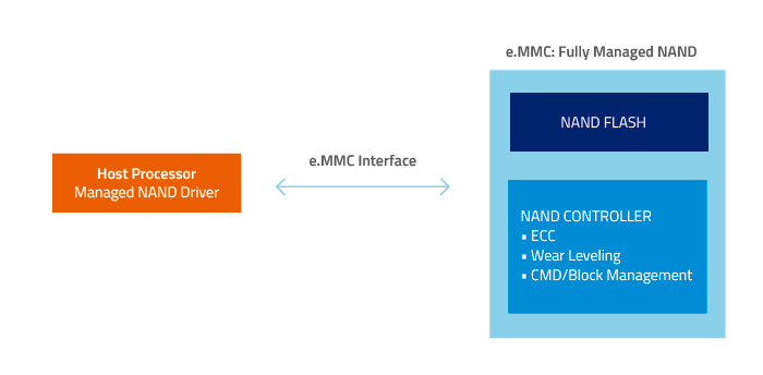
e.MMC Primer
Embedded MultiMedia Controller, or e.MMC, is an advanced managed NAND flash storage solution soldered directly to the motherboard. It integrates the following components in the same IC package:
- MMC interface
- NAND flash memory
- NAND flash controller
In contrast to "raw" NAND solutions like typical solid state drives (SSDs) or SSD modules that require an external hardware controller, e.MMC is "managed" NAND – it combines raw NAND and a sophisticated controller in an integrated package so memory management is done internally.
-
Internal NAND management frees the host from having to perform low-level flash background operations such as wear leveling, bad block management, error correction and other functions.
-
Simplified qualification process reduces time-to-market.
-
High throughput support for large data transfers deliver the performance required by mobile devices.
-
Low power consumption makes the e.MMC a cost-effective solution for space-constrained systems.
-
Simplified memory interface design allows e.MMC to be extremely compact and provides support for future flash storage devices. It is smaller than a postage stamp, making it suitable for automotive and industrial applications requiring rugged endurance, reliability and durability in challenging operating environments.
-
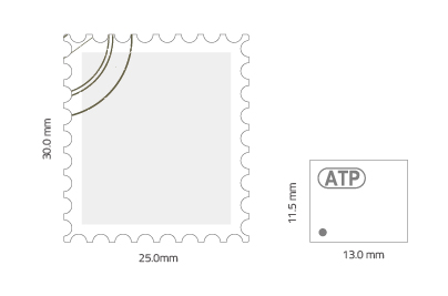
Figure 2. Size comparison between a postage stamp and an e.MMC card.
Usage
e.MMC是一种通用的数据存储和通信介质,并且通常在便携式应用中使用。它的空间占用小,使其成为智能手机,平板电脑和笔记本电脑等移动设备的首选。e.MMC也越来越多地在工业和汽车应用的嵌入式系统广泛使用,例如信息娱乐系统,航空航天/航空电子,物联网(IoT),工业自动化和其他应用。
最新标准
JEDEC在2015年2月发布了最新版本的e.MMC标准。JESD84-B51:嵌入式多媒体卡(e.MMC),电气标准(5.1),也称为e.MMC v5.1,定义了新功能和更新。下表显示了最新e.MMC版本上可用功能的比较。
|
Features |
Version / Year |
||
|
4.51 (2012) |
5.0 (2013) |
5.1 (2015) |
|
|
Max. Bus Speed Mode |
HS200 |
HS400 |
|
|
Max. Data Transfer |
200 MB/s |
400 MB/s |
|
|
Max. Clock Frequency |
200 MHz SDR |
200 MHz DDR |
|
|
Command Queuing |
- |
ü |
|
|
Cache Barrier |
- |
ü |
|
|
Enhanced Data Strobe |
- |
ü |
|
|
Cache Flushing Report |
- |
ü |
|
|
Secure Write Protection |
- |
ü |
|
|
Data Strobe |
- |
ü |
|
|
Data Bus Width* |
4/8 bits |
8 bits |
|
|
Production State Awareness |
- |
ü |
|
|
Field Firmware Update |
- |
ü |
|
|
Device Health Report |
- |
ü |
|
表1 不同e.MMC版本的规格比较
*版本4.51 / 5.0 / 5.1为较低速度(如旧MMC卡,高速SDR和高速DDR)提供向后兼容性时,支持所有数据总线宽度(1/4/8位)。
版本变更要点
|
v4.51 to v5.0 |
v.5.0 to v5.1 |
|---|---|
|
HS400 Mode introduced to enhance sequential read/write performance from 200 MB to 400 MB. |
Command Queuing and Cache Barrier added to enhance random read/write performance. |
|
Production State Awareness (PSA) introduced to secure pre-load data during the e.MMC/PCB soldering process. |
Cache Flushing Report added to ensure the data integrity on cache blocks. |
|
Field Firmware Update (FFU) introduced to allow features enhancement in the field by updating the e.MMC firmware that is fixed on a PCB. |
Enhanced Strobe in HS400 Mode added to facilitate faster synchronization between the host and the e.MMC device. |
|
Device Health Report introduced to monitor the health condition of an e.MMC. |
Secure Write Protection added to ensure that only trusted entities can protect or unprotect the e.MMC device. |
e.MMC v5.1性能
根据JESD84-B51标准,e.MMC v5.1支持以下总线速度和时钟频率。
|
Mode Name |
Data |
I/O Voltage |
Bus Width |
Frequency |
Max. Data Transfer (MB/s, implies x8 |
|
HS400 |
Dual |
1.8/1.2 V |
8 |
0-200 MHz |
400 MB/s |
|
HS200 |
Single |
1.8/1.2 V |
4, 8 |
0-200 MHz |
200 MB/s |
|
High-Speed DDR |
Dual |
3/1.8/1.2 V |
4, 8 |
0-52 MHz |
104 MB/s |
|
High-Speed SDR |
Single |
3/1.8/1.2 V |
1, 4, 8 |
0-52 MHz |
52 MB/s |
|
Backward Compatibility |
Single |
3/1.8/1.2 V |
1, 4, 8 |
0-26 MHz |
26 MB/s |
表2 e.MMC 5.1总线速度模式和时钟频率
与其他NAND闪存产品的比较
e.MMC与其他NAND闪存产品(如固态驱动器(SSD),存储卡和通用闪存(UFS))有何不同? 尽管存储产品都使用NAND闪存芯片,但是它们在物理外观上还有很多不同。
下表信息基于ATP产品规格:
|
Feature |
NAND Flash Product |
|||||
|---|---|---|---|---|---|---|
|
e.MMC |
Memory Cards |
UFS** |
SSD |
|||
|
Protocol |
MMC |
SD |
SCSI |
AHCI (SATA); NVMe |
||
|
Interface |
HS400 |
UHS-I/UHS-II* |
Serial Interface |
SATA; PCIe |
||
|
Form Factor(s) |
153-pin FBGA embedded |
SD/microSD |
Card (removable); BGA (embedded) |
2.5" drives; M.2; eSATA; SlimSATA; mSATA, eUSB |
||
|
NAND Flash Type |
Managed |
Managed |
Managed |
Raw |
||
|
Data Transfer Speed (Max.) |
400 MB/s |
UHS-1: 104 MB/s |
2-lane gear 2: 2-lane gear 3: |
SATA: 550 MB/s PCIe: 32 Gb/s |
||
|
Dimensions |
11.5 x 13 x 1.3 |
SD |
32 x 24 x 2.1 |
11.5 x 13 x 1.0 |
2.5" SSD |
100.0 x 69.9 x 9.2 |
|
microSD |
15 x 11 x 1.0 |
M.2 2242 |
42 x 22 x 3.5 |
|||
|
M.2 2260 |
60 x 22 x 3.5 |
|||||
|
M.2 2280 |
80 x 22 x 3.5 |
|||||
|
SlimSATA |
54 x 39 x 4 |
|||||
|
mSATA |
50.8 x 29.85 x 3.4 |
|||||
|
eUSB |
36.9 x 26.6 x 9.5 |
|||||
表3 e.MMC与其他NAND闪存产品主要区别
* Ultra High Speed bus interface
** UFS availability TBA.
尺寸比较:
The figure below shows the different sizes of ATP flash storage products along with the e.MMC.
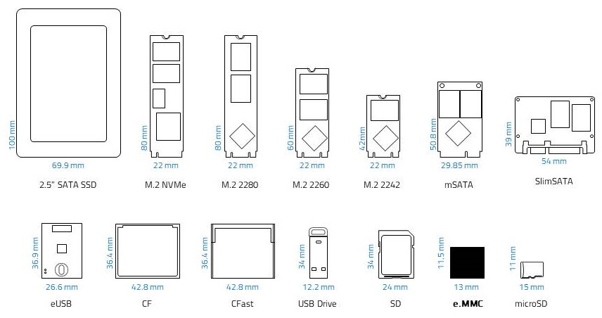
图4 产品尺寸对比
ATP工业/汽车级e.MMC采用153引脚的FBGA封装,旨在满足高性能数据传输,代码和数据存储要求以及汽车级应用(如车载信息娱乐系统) 。 ATP提供的e.MMC产品具有高达128 GB的内存,可用作大容量存储,以实现更高的存储密度。
其e.MMC产品符合JEDEC e.MMC标准v5.1,并与其他e.MMC版本(v4.41 / v4.5 / v5.0)向后兼容。
ATP e.MMC Solutions
|
Product |
e.MMC |
||
|---|---|---|---|
|
Product Line |
Premium |
Superior |
|
|
Naming |
E700Pi |
E600Si |
|
|
IC Package |
153-ball FBGA |
||
|
JEDEC Specification |
v5.1, HS400 |
||
|
Flash Type |
3D SLC Mode |
3D NAND |
|
|
Density* |
8 GB to 64 GB |
16 GB to 128 GB |
|
|
Bus Speed Modes |
x1/x4/x8 |
x1/x4/x8 |
|
|
Performance** |
Sequential Read/Write |
300/220 |
300/220 |
|
Random Read/Write |
15K / 30K |
15K / 30K |
|
|
Operating Temperature |
-40°C to 85°C (industrial) |
||
|
Reliability |
Max. TBW** |
651 TB |
372 TB |
|
MTBF @ 25°C |
> 2,000,000 Device hours |
> 2,000,000 Device hours |
|
|
VCC (Typical RMS in Read/Write) |
130 / 215 |
130 / 215 |
|
|
VCCQ (Typical RMS in Read/Write) |
115 / 105 |
115 / 105 |
|
|
L x W x H (mm) |
11.5 x 13.0 x 1.3 (max.) |
||
表4. ATP工业e.MMC规范
* 1 GB=1,000,000,000 bytes. Actual user storage may be less.
** Based on internal testing; performance may vary depending upon drive capacity, file attributes, host device, OS and application. Cache On.
e.MMC是一种经济,可靠的嵌入式大容量存储设备,将NAND闪存,控制器和接口集成在一个封装中。 ATP提供的e.MMC解决方案能够为需要高性能、高耐用性以及低功耗的应用提供可靠的存储。
想要了解更多,请访问ATP网站或联系ATP代表/经销商。