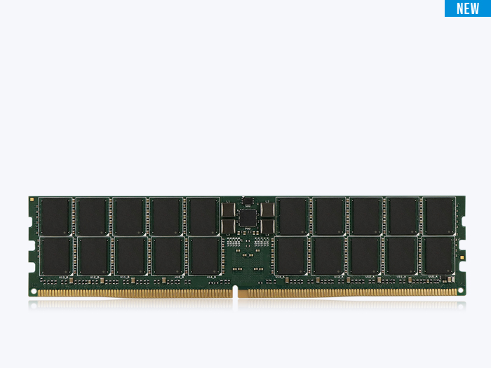
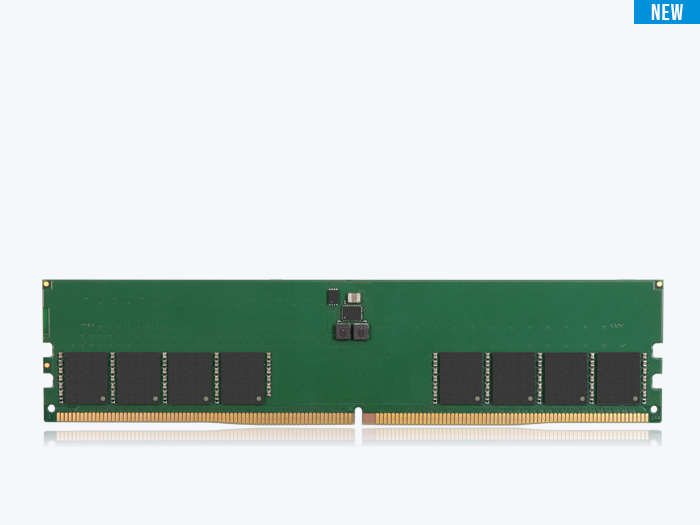
A DDR5 datasheet compresses a module’s entire electrical and logical personality into a few pages — module organization, timings, prefetch, banks, calibration, on-module power, and refresh. This guide walks the fields a design engineer reads most often and explains what each one constrains in a real system.
Key Takeaways
- A DDR5 module organization such as “16Gx80” reports total addressable depth and total bus width, including ECC bits. To get user-accessible capacity, exclude the ECC check bits: 16G × (80 − 16) bits ÷ 8 = 128 GB.
- DDR5 doubled the internal banks to 32, organized into 8 bank groups for x4/x8 devices. Switching between bank groups uses shorter timings (tCCD_S) than staying within one, so the organization directly affects achievable throughput.
- DDR5 uses a 16n prefetch with a default burst length of 16 (BL16). On a 32-bit sub-channel, one BL16 burst transfers exactly 64 bytes — a perfect match for the 64-byte cache line of a modern central processing unit (CPU).
- DDR5 moved voltage regulation onto the module via a PMIC and added on-die ECC. The PMIC steps a 5 V module input down to the core 1.1 V locally, improving signal integrity and removing that regulation burden from the motherboard.
- tCK sets the clock period; data rate is twice the clock frequency. A 6400 MT/s grade runs a 3200 MHz clock, because DDR transfers data on both clock edges.
What a DDR5 datasheet tells you
A DDR5 datasheet packs a module’s entire electrical and logical personality into a few pages of parameters. Most of it carries over conceptually from DDR4, but DDR5 relocated several functions — power regulation, error correction, calibration — and reorganized the memory array. This guide walks the fields a design engineer reads most often, in the order they typically appear, and explains what each one constrains in a real system. For industrial and embedded designs — where ATP builds and validates DRAM — these fields also govern behavior at temperature and duty-cycle extremes a desktop never sees, so reading them precisely is part of specifying for a multi-year deployment.
Throughout, the focus is on the standardized, JEDEC-level meaning of each field — the part that is true of any compliant DDR5 device, independent of vendor.
Module organization and user capacity
DDR5 module organization is written as depth × width across the whole module interface — for example, 16Gx80. The 16G is 16 billion addressable storage locations across the module interface. The 80 is the total data-bus width in bits: a dual-channel (two sub-channel) architecture, each sub-channel 40 bits wide.
Not all 80 bits are user data. In this example, 16 of those bits are ECC check bits, used for reliability and not counted toward user-accessible capacity. The capacity math therefore excludes them:
- 16 billion locations × (80 − 16) data bits = 1024 gigabits
- 1024 Gb ÷ 8 = 128 GB user-accessible capacity
Reading capacity this way — total bus width minus ECC width, times depth — keeps you from over-counting the check bits as usable storage.
Serial Presence Detect (SPD) and the on-module EEPROM
Every DIMM carries a small serial EEPROM (1024 bytes on DDR5) that implements Serial Presence Detect (SPD). SPD is the on-module data store the system reads at boot to learn what the module is and how to drive it. It holds density and configuration, timing parameters (CAS latency, speed grades, refresh requirements), voltage requirements, and identification data such as part number and serial number.
When the BIOS configures memory, it is reading SPD. A correct SPD image is what lets a module train and run at its rated speed without manual tuning.
Clock cycle time (tCK), frequency, and data rate
tCK is the clock cycle time — the average clock period. It relates to frequency inversely: clock frequency f = 1 / tCK. Because Double Data Rate (DDR) memory transfers data on both the rising and falling edges of the clock, the effective data rate is twice the clock frequency, or 2 / tCK.
That factor of two is why the headline numbers and the clock numbers differ. A 6400 MT/s speed grade runs on a 3200 MHz clock; the 6400 megatransfers per second come from using both edges of that 3200 MHz clock.
CAS latency (CL) and speed bins
CAS Latency (CL) — Column Access Strobe Latency — is how long the memory takes to begin delivering data after the controller asks for it, expressed in clock cycles. JEDEC defines DDR5 speed bins as pairs of a data rate (in MT/s) and the CL the controller must wait at that rate.
Because CL is counted in clock cycles, a higher CL number at a higher data rate does not automatically mean more real time — the cycles are shorter. Always evaluate CL together with the data rate it is specified at, not in isolation.
16n prefetch and burst length (BL16)
DDR5 uses a 16n prefetch architecture: for every read or write command, the DRAM core accesses 16 consecutive data words in parallel for each I/O pin, then serializes them for high-speed transmission. The “n” is the number of I/O pins on the chip.
Worked example for an x8 chip (8 I/O pins): a 16n prefetch means the core accesses 16 × 8 = 128 bits internally per request. Those 128 bits are funneled into the I/O buffer and sent across the 8 pins over eight clock cycles, using both edges to move all 16 bits per pin.
The prefetch depth ties directly to burst length. Because DDR5 prefetches 16 words, its default burst length is 16 (BL16). This is not arbitrary — it aligns with modern CPUs, which use 64-byte cache lines. On a standard 32-bit (4-byte) DDR5 sub-channel, one BL16 burst transfers 16 × 4 = 64 bytes, fetching exactly one cache line per burst.
Banks and bank groups
An internal bank is a distinct DRAM cell array that can be accessed independently. DDR5 doubled the bank count from 16 (in DDR4) to 32. Those 32 banks are organized into 8 bank groups, each containing 4 banks (8 × 4 = 32).
The grouping matters for timing. When the controller switches between different bank groups, it can use shorter timings such as tCCD_S, which are faster than the longer timings required when issuing back-to-back accesses within the same group. Spreading traffic across bank groups is therefore a throughput lever, not just a capacity detail.
This 8-group / 32-bank organization is standard for x4 and x8 DDR5 devices, typically used in servers and desktops. By contrast, x16 DDR5 devices — common in laptops and graphics — are usually organized with 4 bank groups and 16 banks total. To locate data, the controller supplies a bank group address, a bank address, a row address, and a column address.
Fly-by topology
Fly-by topology is a routing technique where the command, address, control, and clock signals are linked in series along a single trace that passes each DRAM chip in sequence. Signals travel from the controller (or the module’s register) and reach each chip one after another along that path.
The benefit is signal integrity at high speed: a single, cleanly terminated serial path produces better signal quality than older tree-style routing. Fly-by was introduced with DDR3 and remains standard in DDR5. Its one consequence — the signals arrive at each chip at slightly different times — is corrected by write leveling during initialization.
On-die termination (ODT) and ZQ calibration
On-die termination (ODT) places the termination resistors needed for impedance matching inside the DRAM chip rather than on the motherboard. It is programmable: the resistance values (RTT) are stored in internal Mode Registers and set by the controller during initialization, including distinct values for write operations (RTT_WR). Integrating termination on-die reduces board complexity and helps maintain a stable data eye at high speed.
ZQ calibration keeps that termination — and the output driver strength — accurate over time. DRAM electrical properties drift with voltage and temperature; ZQ calibration corrects the output driver resistance (Ron) and termination resistors (RTT) against a precise external 240-ohm (±1%) reference resistor on the ZQ pin. A periodic short calibration can correct impedance errors as small as 0.5%.
In DDR3 and DDR4, ZQ calibration used dedicated command pins. DDR5 folds it under the Multi-Purpose Command (MPC): the controller issues an MPC with operands that select the calibration task. Moving these functions to the MPC keeps the pin count manageable while supporting a wider set of training and initialization features. Without this calibration, the readable data eye would shrink as the system heats up, eventually causing data corruption — which is why it matters most at the highest data rates.
On-module power: the PMIC
With DDR5, each DIMM includes its own Power Management Integrated Circuit (PMIC). The board delivers a safer 5 V to the module, and the PMIC steps it down locally to the 1.1 V core voltage. Doing regulation on the module has several effects:
- Eliminates IR drop: regulating at the point of use avoids voltage loss along long board traces, keeping the supply precise and stable.
- Improves signal integrity: a shorter electrical path from regulator to chips reduces electrical noise and EMI.
- Finer voltage control: per-module regulation allows granular tuning tailored to that DIMM’s components, which helps high-frequency stability.
- Lowers motherboard cost and complexity: the regulation burden moves off the mainboard.
Refresh: refresh period and tREFI
DRAM cells are capacitors that leak charge, so every row must be refreshed periodically to retain data. The refresh period is the total time allowed to refresh the entire array. For standard operation, every row must be refreshed at least once every 32 ms. Because capacitors leak faster when hot, that window halves to 16 ms in the extended temperature range.
The average refresh interval (tREFI) is the spacing between refresh commands. DDR5 also adds on-die thermal sensing, letting the device hint to the controller via mode registers when a higher refresh rate is needed based on real-time temperature.
Reset and diagnostics: asynchronous reset and connectivity test
Asynchronous reset is a clock-independent mechanism that forces the DRAM into a known, safe initial state by clearing internal registers and state machines. It works even before the system clock is stable, which is essential during power-up, and serves as a recovery tool during errors or instability — placing the device in a protected state (for example, high impedance, ignoring inputs) until normal operation resumes.
Connectivity Test (CT) mode is a low-speed, hardware-based diagnostic that verifies the physical connections between the DRAM and the controller. It reconfigures pins so outputs directly reflect inputs, exposing opens, shorts, and poor solder joints without requiring high-speed operation. Because it runs independently of system timing, CT mode is valuable for debugging non-bootable boards before high-speed training begins.
Frequently Asked Questions (FAQ)
Q1: What does a DDR5 module organization like 16Gx80 mean?
A: 16G is the number of addressable locations across the module; 80 is the total data-bus width in bits, split into two 40-bit sub-channels. Sixteen of those 80 bits are ECC check bits, so user capacity is 16G × 64 ÷ 8 = 128 GB.
Q2: Why is DDR5 burst length 16?
A: DDR5 uses a 16n prefetch, so the core fetches 16 words per request and the default burst length is 16 (BL16). On a 32-bit sub-channel, a BL16 burst moves exactly 64 bytes, matching a CPU’s 64-byte cache line.
Q3: How many banks does DDR5 have?
A: DDR5 x4 and x8 devices have 32 internal banks organized into 8 bank groups of 4 banks each. x16 devices are typically organized with 16 banks in 4 bank groups. More banks allow more parallelism and faster cross-group timings.
Q4: What is ZQ calibration in DDR5?
A: ZQ calibration corrects the DRAM’s output driver resistance and termination resistors against an external 240-ohm reference as voltage and temperature drift. In DDR5 it runs through the Multi-Purpose Command rather than dedicated pins, preserving signal integrity at high data rates.
Q5: Why does each DDR5 DIMM have a PMIC?
A: DDR5 moves voltage regulation onto the module. The board sends 5 V and the on-module PMIC steps it down to 1.1 V locally, which eliminates IR drop along board traces, improves signal integrity, allows finer per-module voltage control, and reduces motherboard complexity.