Industrial SSDs keep NAND flash bit errors and bad blocks from becoming downtime by pairing error correction code (ECC) — Hamming, Reed-Solomon, BCH, and LDPC — with bad block management. This article explains how each algorithm works, why LDPC leads for high-density 3D NAND, and how error correction and failure isolation keep data recoverable in industrial and edge deployments.
Key Takeaways
Industrial SSDs keep NAND flash failures from becoming downtime with two mechanisms working together: bad block management retires blocks that have gone bad, and error correction code (ECC) fixes the bit errors that still-good blocks produce as the flash wears — so a failure is mapped out or corrected before it can corrupt data or stop the system.
- Bad blocks come in two forms. Initial bad blocks ship with a new device and are mapped at the factory; later (accumulated) bad blocks develop in service from program/erase wear, read/write disturb, and retention loss. A bad block table — which the controller keeps in non-volatile flash and loads at boot — keeps both kinds out of the active data path.
- Retiring a block spends the reserve, not the capacity. On a managed device the capacity reported to the host is fixed at design time; when a block is retired, a spare from the reserved pool takes its place. What shrinks is the reserve, and it is finite — so the signal to watch is the drive’s own health reporting, where the product provides it, rather than its capacity.
- ECC corrects bit errors before they become data loss. As NAND scales to smaller geometries and stores more bits per cell, bit errors rise; ECC detects and corrects them in real time, so an aging drive keeps returning correct data instead of failing a read. ATP products use multi-bit ECC, including LDPC, rather than single-bit Hamming codes alone.
- LDPC is the strongest of the four algorithms for modern flash. Hamming corrects a single bit and suits simple SLC designs; Reed-Solomon and BCH correct multiple-bit errors; LDPC additionally uses soft-bit information from the flash and delivers near-capacity performance — which is why it is favored for the high-density TLC and 3D NAND where bit-error rates are highest.
- Error correction does not replace failure management. ECC recovers data from bit errors, but a block with permanent physical damage must be retired, not corrected. Industrial SSDs pair ECC with factory bad-block screening and in-service bad block management, so a failing block is isolated from the active data path rather than corrected indefinitely.
- Not every design needs the strongest ECC. Simple SLC flash with light write loads is well served by single-bit Hamming codes; LDPC’s cost in controller complexity earns its place in high-density TLC/QLC NAND and in long-duration, unattended industrial and edge deployments, where the raw error rate is high and a failed read cannot be tolerated.
Error Detection and Correction in NAND Flash Memory
The current age of information underscores the need, not only of speed but also of accuracy, whether one is storing, retrieving, transmitting or analyzing data. Considering the amount of critical information being generated by the minute, even the slightest of errors can spell disaster. As flash memory moves to smaller geometries, error bits also increase, requiring more powerful error correction algorithms to ensure the reliability of the flash storage device.
Bad Blocks
Bad blocks are blocks that have one or more invalid bits. They may be unusable or weak and prone to errors. They may be present even in new devices and may develop during the lifetime of the device.
There are two types of bad blocks in a NAND flash storage device:
- Initial bad blocks. NAND flash devices may ship out with a number of bad blocks. Before the device is shipped, the location of bad blocks is mapped, and a bad block management algorithm is usually implemented, where a bad block table is created by reading all the spare areas in the flash storage device. Invalid blocks are identified during testing and validation in the factory. The bad block table is saved in a good block, so it can be loaded by the device on reboot (Micron).
- Accumulated or later bad blocks. As the device goes through the rigors of its use, data in the good blocks may be lost or corrupted due to wear out during its lifetime, leading to read/write disturb errors, retention errors, and other issues. Consequently, damaged blocks cause stored data to be inaccessible and applications or operating systems may fail to open. On a managed device the capacity reported to the host does not change as blocks are retired — a spare block from the reserved pool takes over, and it is that reserve which shrinks. The reserve is finite, so the signal to watch is the drive’s own health reporting, where the product provides it, not its capacity.
How Do Industrial SSDs Isolate NAND Flash Failures Before Downtime Occurs?
Industrial SSDs isolate NAND flash failures before they cause downtime by combining bad block management with error correction. The controller retires blocks that have become invalid so no new data is written to them, and ECC corrects the bit errors that still-usable blocks produce as the flash ages, so a read succeeds even on an aging drive. A failure is contained at the block or bit level — mapped out or corrected — long before it can corrupt stored data or halt an application.
The first layer is bad block management, described above. Initial bad blocks are present in new devices; their locations are identified during factory testing and recorded in a bad block table the controller keeps in non-volatile flash and loads at boot. Accumulated (later) bad blocks develop over the drive’s life as program/erase cycling, read and write disturb, and charge-retention loss damage cells that were originally good; these are retired as they appear, and the record of them is persisted as it happens rather than deferred to the next restart. In both cases the bad block management algorithm keeps these blocks out of the active data path, so the storage the host actually uses stays valid — the mechanism that prevents a worn or defective block from silently corrupting data.
The second layer is error correction. Not every degrading cell fails outright; far more often it returns the occasional wrong bit, and the rate of those bit errors climbs as NAND scales to smaller geometries and stores more bits per cell. ECC detects and corrects those errors in real time, so the drive keeps returning correct data while the error rate stays within the code’s correction capability, and bad block management retires a block once it becomes unreliable — keeping it out of the active data path before its errors accumulate into an uncorrectable failure. This matters most in industrial and edge deployments, where a drive often runs unattended at a remote site: a corrected bit error is a non-event, but an uncorrected one can mean a failed boot, a corrupted log, or a service call to a site that no one can reach quickly. ATP pairs this correction with wear leveling, which spreads writes so that no block takes a disproportionate share of the cycling — which delays the point at which bad block management has to intervene at all.
NAND Flash Degradation and Bit Errors
Error correction codes are employed to detect and correct bit errors. In the early days of flash, codes that corrected only a single bit were sufficient, but as scaling became prevalent, cell size decreased and bits per cell increased. The following factors impact flash degradation and the rise of bit errors.
- Program/Erase (P/E) cycles. The constant cycles of programming (writing) and erasing require the application of high voltage to the NAND cell, causing stress on and weakening the Tunnel Oxide.
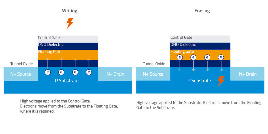
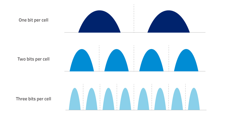
- More bits per cell. In efforts to increase density, new flash technologies have enabled the storing of more bits in a cell, narrowing the gap between voltage threshold (VT) distributions, resulting in voltage shifts and causing bit errors due to cell-to-cell interference.
Error Detection and Correction in ATP NAND Flash Storage Devices
Error correction codes (ECC) are techniques used to correct errors in the NAND flash, allowing recovery of data that may be corrupted due to bit errors. Internal ECC mechanisms can detect and correct up to a certain number of errors.
An example of ECC employed by other flash storage products is the Hamming Code. Invented in 1950 and named after its inventor, Richard Hamming, this algorithm can detect and correct 1-bit errors but can only detect and not correct 2-bit errors. It is easy to implement due to its limited error correcting abilities and is widely used in single-level cell (SLC) flash, which is simpler in architecture and only requires single-bit ECC. A popular Hamming code is 7, 4 where, in a 7-bit block, only 4 bits are made up of data and the other 3 bits are error correction codes.
Below is a sample implementation of the Hamming Code on a 2 KB page with 2048 bytes of user data. In flash storage devices where page size is over 512 bytes, the data is divided into sections of 512 bytes with a Hamming code used for each 512-byte section.
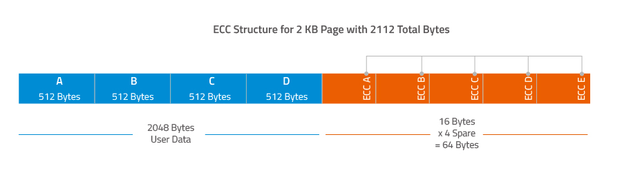
Where a single-bit Hamming code suits simple SLC designs, ATP products employ ECC that corrects multiple bit errors. The following sections introduce the error detection and correction mechanisms applied in ATP’s flash storage devices.
Reed-Solomon Algorithm
Invented in 1960 by engineers Irving Reed and Gustave Solomon, both engineers at MIT’s Lincoln Labs, the Reed-Solomon algorithm involves the addition of extra/redundant data to a block of digital data. It is commonly used in hard disk drives and compact discs, as well as NAND flash storage where it is often used to handle NAND flash bit-flipping. A bit flip occurs when an operation on one cell causes disturbances on another cell due to the proximity of memory cells built too close to each other. When a bit flip happens, the floating gate of a cell may gain (get programmed) or lose (get erased) electrons due to the disturbance in another cell.
Reed-Solomon codes correct symbols and are thus considered excellent for applications where errors tend to be clustered together. The Reed-Solomon algorithm is widely used to correct multiple-bit errors in a single page but may perform poorly with large message blocks, greatly amplifying the time to encode or decode the data when the block size is doubled.
A popular Reed-Solomon code is RS (255, 247) with 8-bit symbols. Each code word contains 255 code word bytes, of which 247 bytes are data and 8 bytes are parity. The decoder can correct any 4 symbol errors in the code word.
Some ATP flash products implement Reed-Solomon encoding that corrects multiple-bit errors within each 512-byte section.
BCH (Bose, Chaudhuri, Hocquenghem) Algorithm
BCH codes were invented in 1959 by Alexis Hocquenghem, and independently in 1960 by Raj Bose and D.K. Ray-Chaudhuri. BCH codes can correct multiple-bit errors and can handle both random and burst errors. The main advantage of BCH codes is that they can be easily decoded using a method called “syndrome decoding.” BCH codes require a low amount of redundancy and are widely used in satellite communications, compact disc drives and bar codes.
In contrast to the Reed-Solomon algorithm, which provides more robust error correction ability but requires a large amount of system resources to implement, the BCH algorithm is becoming popular because of its improved efficiency, being able to detect both highly concentrated and widely scattered errors. Another advantage is that the encoding and decoding techniques are relatively simple and BCH codes require a low amount of redundancy.
LDPC (Low Density Parity Check)
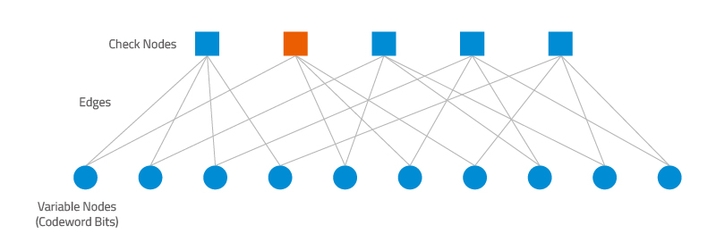
LDPC codes, also known as Gallager codes after their developer Robert G. Gallager, are powerful error-correcting algorithms first introduced in his 1960 doctoral dissertation at MIT (published as a monograph in 1963), but came into wide use only in the 2010s, as controller processing power made their iterative decoding practical. They are increasingly being used in the enterprise world for their ability to decode both soft-bit data and hard-bit data. In Gallager’s thesis, low density parity code is defined as “a linear binary block for which the parity check matrix of interest has a low density of ones,” meaning there are fewer 1s compared to the 0s.
Advantages of LDPC over other algorithms:
- Low decoding complexity
- Uses both hard-bit and soft-bit information from the NAND flash during decoding
- Demonstrates good performance with short blocks
- Delivers “near-capacity” performance with long blocks. (Near capacity refers to the Shannon limit, which is the maximum rate at which data can be sent over a channel with close to or approaching zero error.)
| Bit 1 | Bit 2 | Bit 3 | Bit 4 | Bit 5 | Bit 6 | Bit 7 | Bit 8 | Bit 9 | Bit 10 |
|---|---|---|---|---|---|---|---|---|---|
| 1 | 1 | 1 | 1 | 0 | 0 | 0 | 0 | 0 | 0 |
| 1 | 0 | 0 | 0 | 1 | 1 | 1 | 0 | 0 | 0 |
| 0 | 1 | 0 | 0 | 1 | 0 | 0 | 1 | 1 | 0 |
| 0 | 0 | 1 | 0 | 0 | 1 | 0 | 1 | 0 | 1 |
| 0 | 0 | 0 | 1 | 0 | 0 | 1 | 0 | 1 | 0 |
Table 1. Sample LDPC parity check matrix. Each column is one bit of the codeword — the “Variable Nodes” of Figure 4 — and each row is one parity check.
Summary
The following table provides a comparison of the ECC algorithms discussed in this article.
| Dimension | Hamming | Reed-Solomon | BCH | LDPC |
|---|---|---|---|---|
| Error Correction | Single-bit | Multi-bit | Multi-bit | Multi-bit |
| Flash Type | SLC | MLC | MLC/TLC | TLC / 3D NAND |
| Error Type | Scattered | Burst | Random and burst | — |
| Soft Bit Decoding | No | No | No | Yes |
| Error Correction Capability | Limited | High | High | Very High |
| Performance | Medium | — | High | Very High |
Table 2. Comparison of ECC mechanisms in NAND flash. Ratings are relative to one another rather than absolute measures; a dash marks a dimension this comparison does not rate. (Source: Error Correction Codes in NAND Flash Memory.)
How Does ECC Improve Reliability in Industrial Edge Systems?
ECC improves reliability in industrial edge systems by keeping stored data recoverable even as the underlying NAND flash accumulates bit errors — turning the physical reality that every flash cell eventually produces errors into a corrected read instead of a data-loss event. In an edge system that runs continuously and unattended, that is the difference between a logged, self-healed event and a field failure.
The need for correction grows with the technology. Smaller cell geometries, more bits per cell, and the resulting cell-to-cell interference all raise the raw bit-error rate of modern NAND, which is why the single-bit codes such as Hamming that were adequate for early SLC flash give way to stronger algorithms. Reed-Solomon and BCH correct multiple-bit errors; LDPC goes further, using both hard-bit and soft-bit information from the flash during decoding and delivering near-capacity performance — close to the Shannon limit, the theoretical maximum error-free rate for a channel. The stronger the code, the more margin the drive keeps between its current error rate and the point of uncorrectable failure — margin that a long-lived edge deployment spends gradually as the flash wears.
Edge conditions make that margin valuable. Devices are deployed for years, cycled hard, and often exposed to temperature swings and power quality a data center never sees, all of which push the bit-error rate up over time. Multi-bit ECC absorbs that drift, so the drive keeps meeting its reliability targets deep into its service life. The honest boundary is that ECC is not free: stronger codes cost controller complexity and some decode latency, so the algorithm should match the flash — simple Hamming ECC still suits light-duty SLC designs, while LDPC earns its place in the high-density TLC and 3D NAND used in capacity-hungry edge and industrial storage. ATP applies multi-bit ECC across its industrial SSDs, e.MMC, and industrial memory cards for exactly this reason.
Why Reads Slow Down Before Anything Fails
The cost of correction does not arrive where most engineers expect it. On a page the controller reads cleanly, decoding is a fixed step in the read path; it does not get slower as the flash wears. What changes is how often the first attempt comes back too noisy to decode.
When that happens, the controller does not push harder on the code. It goes looking for a better reference voltage, re-reading the page at adjusted voltage settings until one comes back clean enough to decode. Each of those is another attempt at the same page. The drive returns correct data, and takes longer doing it. On drives that offer it, ATP’s Auto-Read Calibration works the same problem from the other side: as cells age and the voltage levels they hold drift away from the thresholds the controller reads them against, ARC recalibrates those thresholds rather than leaving them fixed.
Two different things push that retry count up, and it is worth being able to tell them apart.
The first is wear. Years of program/erase cycling, disturb and retention loss shift the voltage levels the cells hold away from the thresholds the controller reads them against, raising the raw bit error rate of the flash itself, so more reads come back needing a second look. This driver is permanent and climbs slowly over months.
The second has nothing to do with age. Signal integrity — keeping data signals clean as they travel through the controller, the NAND interface and the PCB traces — degrades when temperature swings and electrical noise narrow the timing margins those signals depend on. A drive in a rail-side cabinet in February and the same drive on a factory floor in August are not reading under the same conditions. Retries climb, latency climbs with them, and not one cell has degraded. This driver is reversible. Wear is not.
The second driver is the one a drive can be designed to absorb. AcuCurrent, ATP’s signal-integrity optimization technology for its NVMe SSDs, adjusts drive settings in real time during cold boot and under sustained load as temperature changes, which reduces the need for read-retry cycles in the first place — the same idea as a camera’s auto-exposure adapting as you step from a dark room into daylight, so every shot comes out consistent rather than exposed for somewhere the camera no longer is. In an ATP lab evaluation on PCIe Gen4 NVMe E1.S drives held at 70°C, four drives on fixed settings logged 240, 6, 622 and 687 read-retries over the same time window, and zero on temperature-responsive settings — illustrative results, not a performance claim, and results vary by workload, configuration and platform.
Where this does not apply. None of this buys endurance. Read Retry and, on drives that offer it, Auto-Read Calibration recover the read; AcuCurrent keeps the signal clean across temperature so fewer reads need recovering. Not one of them returns a spent P/E budget — a drive at the end of its rated cycling is at the end of it, however well it is tuned. And if your storage sits in a climate-controlled rack that never sees a thermal swing, the thermal driver is not your binding constraint — a standard drive may well be the right specification, and wear is the number to watch.
For a design engineer, the practical consequence is which number to watch. Read-retry counts and the drive’s own health reporting show where the margin has gone. Reported capacity and failure counts stay flat until the margin is already gone.
Conclusion
As NAND flash lithography scales down, cell geometries shrink and cells store more bits per cell; densities increase but so do error bits. To ensure the reliability of its industrial flash storage products, ATP employs multi-bit error detection and correction technologies. For more information about ATP’s high-performance and high-reliability products, visit the ATP website or contact an ATP Representative in your area.
Frequently Asked Questions (FAQ)
Q1: How do industrial SSDs isolate NAND flash failures before downtime occurs?
A: Industrial SSDs isolate NAND flash failures using two layers that work together. Bad block management retires blocks that have become invalid — whether they shipped bad or wore out in service — by keeping them in a bad block table the controller keeps in non-volatile flash and loads at boot, so no data is written to them. Error correction code (ECC) then corrects the bit errors that still-good blocks produce as they age, so reads keep succeeding while the error rate stays within the code’s capability. Bad block management retires a block once it becomes unreliable, keeping it out of the active data path before its errors accumulate into an uncorrectable failure. The result is that a flash failure is contained — mapped out or corrected — before it reaches the host as data loss or a crash. Wear leveling complements this by spreading writes evenly, so no block takes a disproportionate share of the cycling.
Q2: How does ECC improve reliability in industrial edge systems?
A: ECC (error correction code) improves reliability in industrial edge systems by keeping stored data recoverable even as NAND flash accumulates bit errors over years of continuous, unattended operation. Every flash cell eventually returns occasional wrong bits, and the rate rises as cells shrink and store more bits per cell; ECC detects and corrects those errors in real time, so a bit error becomes a corrected read instead of a data-loss event or a failed boot at a remote site. Stronger algorithms keep more margin between the drive’s error rate and the point of uncorrectable failure — margin a long-lived edge deployment spends gradually as the flash wears. ATP uses multi-bit ECC, including LDPC, rather than single-bit codes alone.
Q3: What is the difference between BCH and LDPC error correction in SSDs?
A: BCH and LDPC are both multiple-bit error-correcting codes, but they differ in how they decode. BCH decodes with hard-bit information — each cell is read as a firm 0 or 1 — which keeps it simple and low in redundancy, and it handles both random and burst errors well. LDPC can additionally use soft-bit information, a probability that a bit is 0 or 1, to recover data at higher error rates, and it delivers near-capacity performance (close to the Shannon limit, the theoretical maximum error-free rate for a channel). That extra headroom is why LDPC is favored for high-density TLC and 3D NAND, where raw bit-error rates are highest, while BCH remains a good fit for less demanding designs.
Q4: Why does NAND flash need stronger error correction as it scales down?
A: As NAND flash lithography scales to smaller geometries, two things happen at once: cells are packed more closely, increasing cell-to-cell interference, and manufacturers store more bits per cell, which narrows the voltage margins that separate one stored value from another. Both effects make bit errors more likely, and program/erase cycling adds to them by stressing and weakening the cell’s tunnel oxide over the device’s life. Early flash could rely on single-bit codes like Hamming; today’s high-density flash needs multi-bit algorithms such as Reed-Solomon, BCH, and especially LDPC to keep the growing number of bit errors correctable and the stored data reliable.
Q5: What are bad blocks in NAND flash, and how does an SSD manage them?
A: A bad block is a NAND flash block with one or more invalid bits, which may be unusable or simply unreliable. Some are initial bad blocks present in a new device; others accumulate over the device’s life as wear, read/write disturb, and retention loss damage previously good blocks. An SSD manages them with a bad block table the controller keeps in non-volatile flash and loads at boot: invalid blocks are identified during factory testing and as they develop in service, recorded in the table, and kept out of the active data path. Left unmanaged, bad blocks would let stored data become inaccessible. On a managed device they do not shrink the capacity reported to the host — a spare replaces each retired block, so what shrinks is the reserve the drive holds for that purpose.
Q6: Why is my SSD getting slower to read but not failing?
A: Rising read latency on a drive that still returns correct data is usually read-retry, not extra error-correction work. Decoding a clean page is a fixed step in the read path and does not get slower as the flash wears; what changes is how often the first read attempt comes back too noisy to decode. The controller then goes looking for a better reference voltage, re-reading the page at adjusted voltage settings until one comes back clean enough to decode; each of those is another attempt at the same page, so the read succeeds and takes longer doing it. On drives that offer it, ATP’s Auto-Read Calibration works the same problem from the other side, recalibrating the read thresholds as the voltage levels the cells hold drift with age. Two things push that retry count up: wear, which is permanent, and loss of thermal and electrical margin, which is not. Read-retry counts and the drive’s own health reporting show where the margin has gone; reported capacity and failure counts stay flat until it is already gone.