In some cases, DRAM modules may show incorrect total memory values in the BIOS/UEFI interface, while operating correctly in the operating system. This issue often stems from compatibility problems between the module's SPD data and the BIOS/UEFI firmware. This article addresses a specific issue observed with DDR5 DRAM modules, explaining the underlying causes and reassuring customers about the implications, Terms and Definitions
BIOS. This stands for "Basic Input/Output System." It is firmware stored on a small memory chip on the system motherboard. It loads the operating system and performs an initial pack of diagnostic tests on system hardware components.
UEFI. This stands for “Unified Extensible Firmware Interface.” It is specification for a software application that links the operating system (OS) and firmware of a computer. UEFI is eventually intended to replace BIOS but is compatible with it. UEFI runs in 32- or 64-bit mode and provides a more sophisticated graphical user interface than BIOS, which has a limited user interface and uses 16-bit mode.
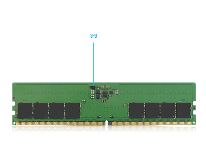
SPD. This stands for “Serial Presence Detect.” It is a memory hardware feature that allows the computer to determine what memory is available and what timings to use to access it.
POST. This stands for “Power-On Self-Test.” It is one of the initial diagnostic tests performed by the BIOS/UEFI when the computer is powered on to ensure that all hardware components are functioning properly
Issue Overview
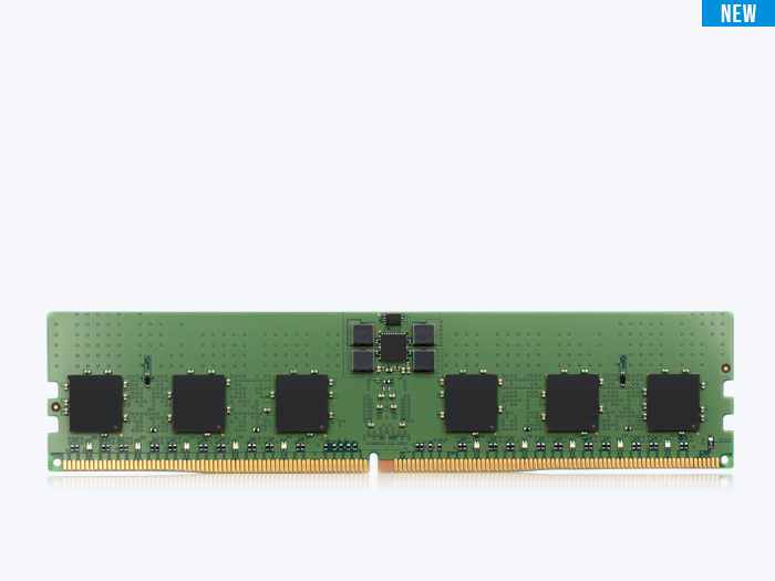
Recently, it was observed that ATP DDR5 DRAM modules were displaying "0GB" as the total memory in the BIOS/UEFI menu, despite functioning correctly and showing the correct capacity in the operating system (e.g., Windows). After a thorough analysis, it was determined that this issue was due to the Manufacturer ID in the SPD (Serial Presence Detect) not being recognized by the BIOS/UEFI.
Understanding the SPD Data
The SPD data contains crucial information about the DRAM module, including timing parameters, module type, and density. The SPD data is accessed by the BIOS/UEFI during system startup to correctly configure and utilize the memory.
BIOS/UEFI and SPD Data Interaction
How BIOS/UEFI Reads SPD Data
- SPD Data Access: During the POST (Power-On Self-Test) process, the BIOS/UEFI reads the SPD data from the DRAM modules to configure them correctly.
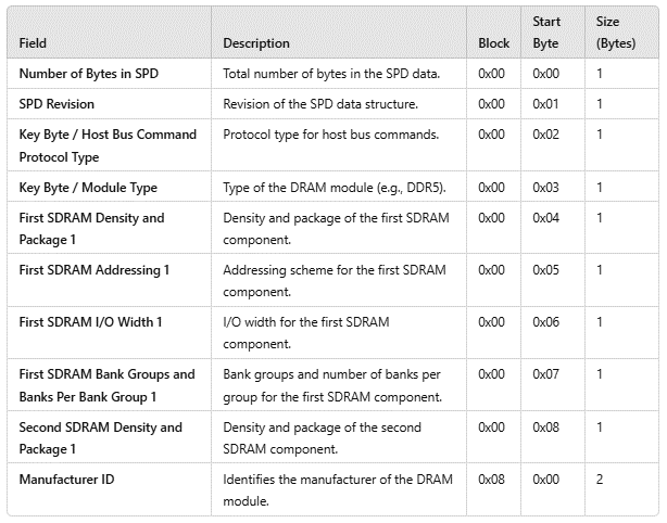
- Manufacturer ID: The BIOS/UEFI checks the Manufacturer ID in the SPD to identify and configure the module. If the Manufacturer ID is not recognized or is missing, the BIOS/UEFI might not display the correct total memory.
- Calculation of Total Memory: The BIOS/UEFI calculates the total memory based on the individual module capacities read from the SPD. If there's an issue with recognizing the Manufacturer ID, this calculation might be incorrect.
Impact of the Issue
- Total Memory Display: The issue with displaying "0GB" in the BIOS/UEFI menu is a cosmetic and configuration problem rather than a functional one.
- System Functionality: Despite the incorrect total memory display in the BIOS/UEFI, the modules function correctly, and the operating system recognizes and utilizes the full capacity of the installed memory.
Detailed Technical Information
SPD Key Fields
Example: Calculating DRAM Module Capacity
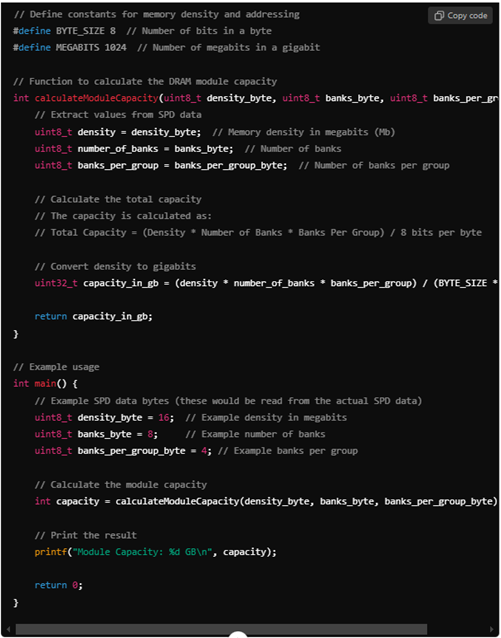
The capacity of a DRAM module can be calculated using the information stored in the SPD (Serial Presence Detect) data. Below is a C-like pseudocode example that demonstrates how to compute the total capacity of a DRAM module based on the data fields specified in the JEDEC standards.
Pseudocode for Capacity Calculation

Explanation
- Density Byte: Represents the density of the DRAM chip in megabits.
- Banks Byte: Indicates the number of banks in the DRAM module.
- Banks Per Group Byte: Specifies the number of banks per group in the DRAM module.
In this pseudocode:
- Density: Extracted from the SPD chip density byte.
- Number of Banks: Extracted from the SPD banks byte.
- Banks Per Group: Extracted from the SPD banks per group byte.
The total capacity is calculated by multiplying these values and dividing them by the number of bits per byte, converting the result to gigabytes.
Conclusion
The issue with DDR5 DRAM modules displaying "0GB" as the total memory in BIOS/UEFI is attributed to a recognition problem with the Manufacturer ID in the SPD data. However, this does not affect the functional performance of the modules, which operate correctly and are recognized by the operating system. By understanding the interaction between SPD data and BIOS/UEFI, users can address compatibility issues and ensure optimal system performance.

