Every Dynamic Random Access Memory (DRAM) module is expected to perform reliably for years under heat, corrosive contaminants, and electrical stress. This article explains what shortens DRAM lifespan — and how ATP’s stringent two-level test flow, from IC-level screening to module-level ATE and Test During Burn-In (TDBI), forces weak chips to fail before they ever ship.
Key Takeaways
- Four factors shorten DRAM lifespan in continuous-operation industrial systems: sustained heat that accelerates charge leakage in DRAM cells and erodes timing margins; corrosive contaminants such as sulfur, which converts the silver in chip resistors into non-conductive silver sulfide; electrical stress from ESD and power surges; and marginal ICs that pass a brief room-temperature test but fail in early life.
- Consumer RAM fails in industrial embedded systems because it is rated and tested for a different environment. Commercial-grade modules operate from 0°C to 85°C and are functionally tested at room temperature — adequate for a desktop PC, not for a sealed cabinet that runs 24/7 through cold starts, heat, and contaminated air.
- Screening is the only defense against early-life failures. Following the bathtub curve, weak chips fail disproportionately in their first months of service. ATP screens ICs at low and wide temperatures before assembly, then burns in modules with Test During Burn-In (TDBI) across a −40°C to 85°C chamber ambient range to force those failures out before shipment.
- Not every embedded system needs industrial-grade DRAM. If the enclosure is climate-controlled, stays within 0°C to 85°C, and a failed module is easy to reach and replace, commercial-grade memory is adequate and costs less.
Why DRAM Module Reliability Matters
On every Dynamic Random Access Memory (DRAM) module are multiple memory ICs, each containing billions of memory cells that are expected to perform reliably over long stretches of time under tough workloads and settings. Whether at rest or in operation, these modules face hazards throughout their usage life, and any malfunction can lead to system breakdowns that could disrupt or delay business operations. As such, these components should be manufactured and packaged according to very high standards, and their use should be managed in such a way that would address or minimize known risks.
Challenges
As ICs continue to diminish in size, they become more susceptible to damage from a host of environmental factors, especially for systems placed in inhospitable locations with severe hot or cold temperatures and airborne particles. Systems set up in outdoor remote areas where access to regular maintenance is limited are particularly vulnerable.
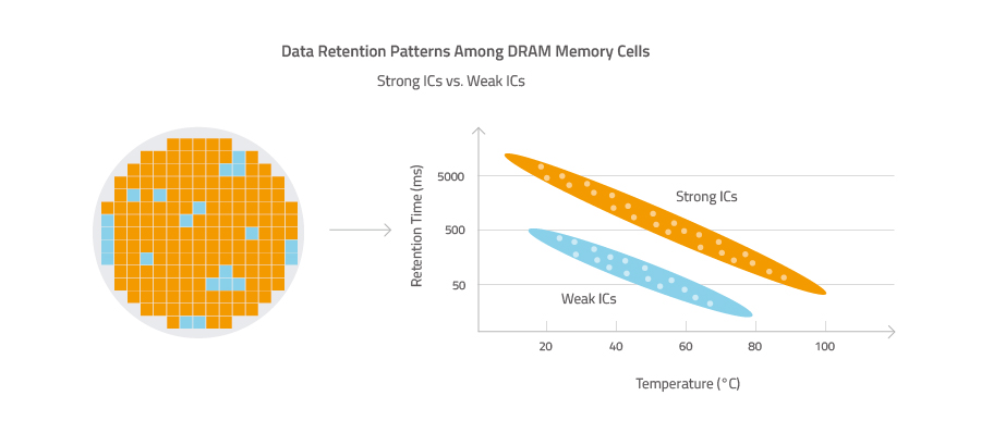
- Uneven IC Quality. ICs within a wafer may not all have the same quality. There may be strong and weak ICs in one wafer. When different-quality ICs are used on the same DRAM module, the module will cause unstable system operation.
- Thermal. High operating temperature can cause DRAM chips to degrade fast, especially when installed in systems and environments with poor air flow.
- Environmental. Particles such as dust, harmful gases, aggressive chemicals, humidity, water and other airborne elements that penetrate the DRAM module can cause corrosion and damage. For example, when sulfur from the environment enters gaps in the resistors and comes into contact with silver, the chemical reaction converts the conductive silver into silver sulfide, a non-conductive compound — the resistor goes open circuit and the module fails (see Protected from Corrosive Sulfur below for the full mechanism and countermeasure).
- Electro-Mechanical. Damage to the contacts/gold fingers can weaken or adversely impact signal integrity. Friction or contact between surfaces transfers electrons and builds up electrostatic charge; when that charge suddenly discharges through a component — an electrostatic discharge (ESD) event — even small parametric shifts can degrade performance or destroy the device. The simple unwinding of tape from a roll or walking on a carpet can generate static electricity, with friction, contact area and humidity determining the amount generated. A power surge or spike, which delivers a sudden power voltage increase, could also be harmful to the ICs or memory chips, causing the DRAM to malfunction or shortening its useful life. Voltage fluctuations and sudden power loss events can degrade components and circuits, reduce equipment life and cause data loss or corruption.
What Reduces DRAM Lifespan in Continuous-Operation Industrial Systems?
Four factors account for most DRAM lifespan loss in systems that never power down: sustained thermal load, corrosive contaminants, electrical and mechanical stress, and marginal ICs that were never screened out.
- Sustained heat. A system that runs continuously holds its memory at operating temperature with no cool-down window. Heat accelerates charge leakage in DRAM cells and erodes timing margins, so marginal devices begin producing intermittent errors long before they fail outright — and poor enclosure airflow compounds the effect.
- Corrosive contaminants. In sulfur-heavy environments — mines, petrochemical plants, polluted industrial zones — airborne sulfur reacts with the silver electrodes in chip resistors, converting the conductive silver into non-conductive silver sulfide. The resistor goes open circuit and the module fails. Humidity and dust accelerate the same corrosion paths.
- Electrical and mechanical stress. Static charge built up by friction or contact discharges through the module as ESD; power surges and voltage fluctuations degrade circuits cumulatively; and worn edge-connector contacts weaken signal integrity with every insertion cycle.
- Marginal ICs. A chip that passes a brief room-temperature functional test can still fail within its first months under sustained thermal and electrical load. Because a module carries multiple DRAM ICs, even a very small marginal rate per chip compounds into a meaningfully higher failure rate at module level.
The first three factors are countered in hardware — conformal coating, anti-sulfur resistors, and thicker gold-finger plating, covered below. The fourth can only be addressed by screening: stressing every chip and module until the weak ones reveal themselves before shipment, which is exactly what the two-level test flow in the next section is built to do.
Reliability Solutions and Technologies
DRAM modules for the enterprise and industrial markets are typically installed in high-performance environments such as data centers where non-stop computing is done on massive scales and any disruption in operation can impact business heavily. Usage in IoT systems is also common. These systems may be situated in remote places that could be difficult to reach for regular maintenance. It is therefore important to make sure that the DRAM modules can be depended on for long stretches of time.
ATP’s modules undergo two levels of testing to ensure maximum reliability:
- Advanced IC-Level Testing screens for ICs with the best reliability and quality characteristics that are suitable for applications requiring wide temperature.
- Enhanced Module-Level Tests: Test During Burn-In (TDBI) and Automatic Test Equipment (ATE) guarantee that modules meet and even exceed qualifying parameters.
IC-Level Testing
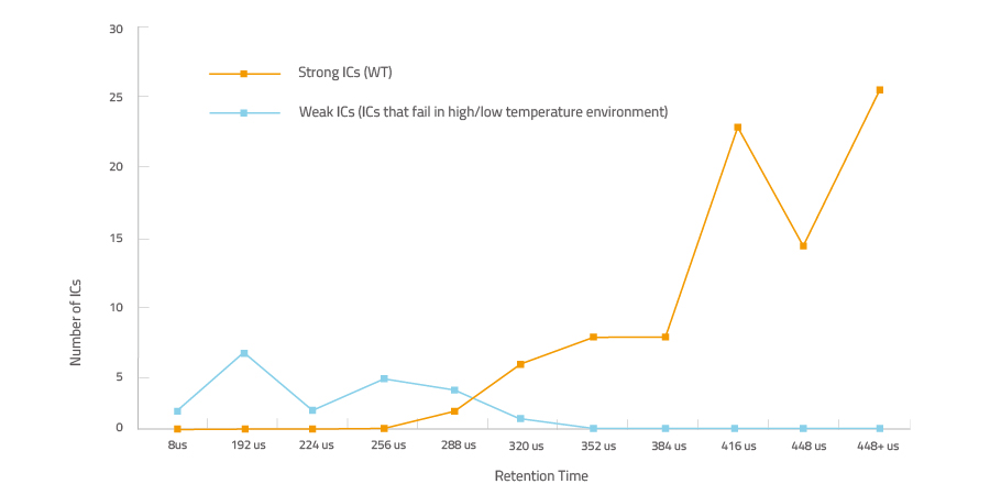
It is extremely important to determine the electrical and mechanical characteristics of individual components that will be used on ATP’s DRAM modules to ensure the highest quality and reliability. IC-level testing is conducted to ensure the reliability of the new die, and the ICs are subjected to low and wide temperature tests to screen out weak ICs.
Module-Level Testing
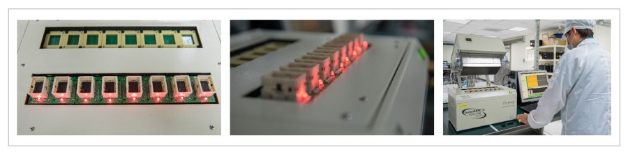
- Functional Testing Using Automatic Test Equipment (ATE). The ATE detects component defects and structural defects related to the DIMM assembly and screens out marginal timing and signal integrity (SI) sensitivities. ATE provides electrical testing patterns with various parameter settings, such as marginal voltage, signal frequency, clock, command timing and data timing under continuous thermal cycle. Also, based on customers’ requests, tailor-made electrical testing patterns can be programmed and implemented into the ATE testing process. The ATE testing system can pinpoint individual defective ICs or DRAM PC boards, thus providing a more efficient failure analysis method for both new product development and mass production stages.

- System-Level Failure Detection and Prevention via TDBI. The bathtub curve in Figure 5 illustrates the three key periods of product failure. High failure rates occur during the early life or infancy, but go down to a constant rate during the normal usage life. Failure rates increase again as the product wears out and approaches the end-of-life stage.
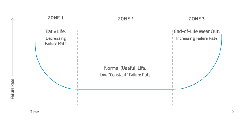
Test During Burn-In (TDBI) at mass production level detects early life failures (ELF) and effectively screens out weak ICs that could fail during the early product life.
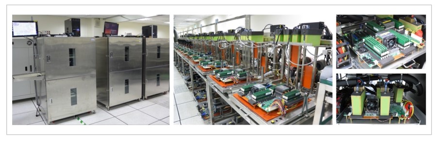
The ATP TDBI system applies extreme high/low temperature, high-low voltage, and pattern testing on DRAM modules. The system consists of:
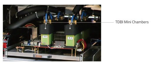
- The miniature chamber, which isolates temperature cycling only to the module being tested so as not to thermally stress the rest of the testing systems. This minimizes the failure of other testing components, such as the motherboards. In conventional large thermal chambers, the failures of non-DRAM-related testing components are constant given that the whole system is thermally stressed.
- Module riser adapters from the motherboard, which allow easy module insertions in production-level volumes.
- Multiple temperature sensors, which regulate temperature profiles across a chamber ambient range of −40°C to 85°C.
A module carries multiple DRAM ICs, so even a very small marginal-failure rate per chip compounds into a meaningfully higher failure rate at module level. Through accelerated testing methods such as TDBI, ATP screens out these marginal chips before shipment — lowering field failure rates and extending service life by making sure that only robust DRAM chips are on the module.
ATP DRAM Special Features
- Thermal Tolerance. ATP DRAM modules with industrial temperature rating can endure extreme temperatures ranging from −40°C to 85°C, ensuring long-term stability for systems installed in telecom, industrial and defense/aerospace operations where consistent availability and steadfast performance are of critical importance.
- Sealed Against the Elements. ATP seals its modules with a parylene conformal coating — a polymer film deposited by chemical vapor deposition (CVD) that “conforms” to every surface. The film shields against dust, chemicals, extreme temperatures, moisture and corrosion. Unlike dipping and spraying techniques, the CVD process is completely pinhole free, as the film conforms to any irregular shape, coating all components and potential points of failure. The parylene film provides exceptional rust prevention; resistance to solvents, acids and alkalis; excellent insulation and dielectricity; and high tensile and yield strength.
- Protected from Corrosive Sulfur. Silver is the most widely used conductive material for sensitive electronic parts such as electrodes in chip resistors. Among all the metals, pure silver has the highest electrical and thermal conductivity. It is also resistant to oxidation, which is a form of metal corrosion. However, when sulfur-containing particles from the environment are diffused or enter gaps in the resistors and come into contact with silver, the chemical reaction that follows transforms the conductive silver-based electrode into a non-conductor called silver sulfide. When silver corrodes, it loses conductivity; the resistor then goes open circuit and will no longer function properly, ultimately leading to module failure. High sulfur concentration is found particularly in mines, petrochemical plants and polluted industrial areas; where oil, gas lubricants or fossil fuels are used; geothermal/volcanic sites and hot springs; and waste disposal sites. ATP DRAM modules use anti-sulfur resistors (on a project basis) that repel the damaging effects of sulfur contamination, guaranteeing continued dependable performance and lowering the total cost of ownership by preventing unnecessary downtime and expensive component replacements.
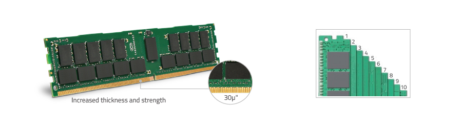
- Thicker Gold Fingers and PCB. Gold fingers are the gold-plated edge connector contacts on the DRAM printed circuit board (PCB). They are referred to as such because they are long and narrow, resembling fingers, and are gold-plated to help protect the PCB from wear and tear. To ensure the quality of the signal transmission between the connector and the ATP DRAM module, ATP utilizes gold-finger plating with 30µ" thickness, while thinner plating is common on commercial-grade modules. Additionally, the module is built on a 6- to 10-layer printed circuit board (PCB), ensuring better signal quality as well as module durability for many years of reliable use.
Why Does Consumer RAM Fail in Industrial Embedded Systems?
Consumer RAM fails in industrial embedded systems because it is rated, tested, and built for a different environment: an office-ambient PC that idles most of the day and can be rebooted or swapped in minutes. Drop the same module into an unattended embedded system running 24/7 and three gaps surface:
- The rating gap. Commercial-grade modules operate from 0°C to 85°C. Industrial embedded systems live in fanless boxes, outdoor cabinets, and vehicles that swing outside that band on both ends — a module rated to 0°C cannot be trusted to cold-start below freezing, and sustained heat near the upper limit accelerates degradation.
- The screening gap. A consumer module that passed a room-temperature functional test can still carry marginal ICs. In a desktop, an early-life failure means a reboot or an RMA; in an embedded controller, it means unplanned downtime and a site visit. ATP screens ICs at low and wide temperatures before assembly and stresses every module with Test During Burn-In (TDBI) — combined temperature, voltage, and pattern stress at chamber ambient temperatures from −40°C to 85°C — to remove weak parts before they ship.
- The hardware gap. Consumer modules carry no defense against contaminated or humid air. ATP industrial modules add a pinhole-free parylene conformal coating applied by chemical vapor deposition, anti-sulfur resistors (on a project basis), 30µ" gold-finger plating, and 6- to 10-layer PCBs for signal quality and durability.
| Dimension | Consumer / Commercial-Grade DRAM | ATP Industrial DRAM |
|---|---|---|
| Operating temperature | 0°C to 85°C | −40°C to 85°C industrial temperature rating |
| IC screening | IC vendor’s standard production test | Additional low- and wide-temperature IC-level screening before assembly |
| Module testing | Room-temperature functional test | ATE (marginal voltage, timing, and signal integrity under thermal cycling) plus TDBI burn-in at −40°C to 85°C chamber ambient |
| Environmental protection | None | Parylene conformal coating; anti-sulfur resistors (project basis) |
| Connector and PCB | Standard plating and layer count | 30µ" gold-finger plating; 6- to 10-layer PCB |
None of this means consumer memory is poorly made — it is qualified for the environment it was designed for. If your embedded system sits in a climate-controlled enclosure that stays within 0°C to 85°C and is easy to service, commercial-grade memory is adequate and costs less. The case for industrial-grade — including DDR5 wide-temperature modules — becomes compelling the moment temperature, air quality, or site access is no longer under your control.
Conclusion
Reliable DRAM is not an accident of good components — it is the outcome of a test flow that screens ICs before assembly and stresses every finished module until weak parts reveal themselves. ATP has more than 30 years of expertise in manufacturing industrial-grade memory and storage products. Visit the ATP website for more information on which DRAM solutions are best suited for your industrial and embedded requirements, or contact an ATP Distributor/Representative in your area.
Frequently Asked Questions (FAQ)
Q1: What reduces DRAM lifespan in continuous-operation industrial systems?
A: Four factors: sustained heat, corrosive contamination, electrical stress, and marginal ICs. Continuous operation holds the module at sustained temperature, accelerating charge leakage in DRAM cells and eroding timing margins; airborne sulfur converts the silver electrodes in chip resistors into non-conductive silver sulfide, causing open circuits; electrostatic discharge and power surges degrade circuits cumulatively; and chips with marginal quality fail disproportionately in early life under continuous load. Industrial DRAM counters all four with IC-level temperature screening, module-level ATE and TDBI burn-in testing, parylene conformal coating, and anti-sulfur resistors.
Q2: Why does consumer RAM fail in industrial embedded systems?
A: Consumer RAM fails in industrial embedded systems because it is rated and tested for office conditions, not continuous operation in uncontrolled environments. Commercial-grade modules operate from 0°C to 85°C and receive room-temperature functional testing, so a module can ship with marginal ICs that pass a brief test yet fail early under sustained thermal and electrical load. Industrial embedded systems add sub-zero cold starts, corrosive or humid air, and unstable power that consumer hardware carries no protection against. Industrial DRAM modules are rated −40°C to 85°C, screened at IC level, burn-in tested across a −40°C to 85°C chamber ambient range, and available with conformal coating and anti-sulfur resistors.
Q3: What is Test During Burn-In (TDBI) for DRAM?
A: Test During Burn-In (TDBI) is a mass-production screening process that applies extreme high and low temperatures, high and low voltages, and test patterns to DRAM modules over an extended period, forcing early-life failures to surface before modules ship. Product failures follow a bathtub curve — highest during early life, low and constant through normal service, rising again at wear-out — so screening out the weak chips responsible for early-life failures is what flattens the front of the curve. ATP’s TDBI system uses miniature thermal chambers that isolate temperature cycling, across a chamber ambient range of −40°C to 85°C, to the module under test, so results are not distorted by thermal stress on the surrounding test hardware.
Q4: What is the difference between IC-level and module-level DRAM testing?
A: IC-level testing qualifies individual DRAM chips before assembly, using low- and wide-temperature screening to remove weak ICs from the supply. Module-level testing validates the assembled module: automatic test equipment (ATE) detects component and assembly defects and screens marginal voltage, timing, and signal-integrity behavior under continuous thermal cycling, while TDBI burn-in stresses the complete module over time to catch early-life failures. Both levels are necessary — a module built from good ICs can still fail from an assembly defect, and a very small marginal rate per chip still compounds across the multiple ICs on one module.
Q5: Do all embedded systems need industrial-grade DRAM?
A: No. If the system operates in a climate-controlled enclosure that stays within 0°C to 85°C, power is stable, and a failed module is easy to reach and replace, commercial-grade DRAM — such as ATP’s Momentum line — is adequate and costs less. Industrial-grade DRAM earns its premium where temperature is uncontrolled or drops below freezing, the air is corrosive or humid, the site is remote or unattended, or downtime is unacceptable.