By evenly distributing program/erase (P/E) cycles among all blocks, wear leveling extends the lifespan of industrial SSDs, SD/microSD cards and e.MMC — here's how dynamic, static and global wear leveling work, and what they mean for rated endurance.
Key Takeaways
- Wear leveling extends flash storage lifespan by distributing program/erase (P/E) cycles evenly across all NAND blocks, so no block wears out prematurely while others sit nearly unused. It runs in the device's flash controller, independent of the host system.
- In an industrial SSD, wear leveling is what makes the endurance rating real. A TBW figure assumes the controller can spend the P/E cycles of every block, not just the frequently written ones. ATP's global wear leveling manages all NAND in the drive as one pool, supporting sequential-rated endurance up to 20,480 TB written in 3D TLC and 59,250 TB in pSLC mode on its 2.5" SATA line, which carries a separate rating of 1 drive write per day (DWPD) for 5 years under enterprise (random) workload.
- Wear leveling matters even more in a microSD card than in an SSD. A card has far fewer NAND dies and much less spare area than an SSD, so write hot spots — file allocation tables, loop-recording metadata — would otherwise exhaust a handful of blocks while the rest of the card sits idle. ATP's industrial microSD cards run the same advanced wear leveling in the card controller, supporting ratings up to 5,500 TB written in 3D TLC and 12,670 TB in pSLC mode.
- The three types differ in coverage: dynamic wear leveling levels only free blocks; static wear leveling adds blocks holding rarely changed ("cold") data; global wear leveling extends coverage across every die in the device. ATP Enhanced Wear Leveling combines all three.
- Wear leveling cannot add endurance the NAND doesn't have. If your workload will exceed the device's rated TBW — a figure measured under sequential writes, which random workloads reach sooner — the answer is higher-endurance flash (pSLC or SLC) or more capacity, not a better algorithm.
NAND flash cells are arranged in pages and blocks. Data is written on pages, but the minimum unit of erasing is by blocks. Due to the nature of flash, the cells wear out with each program and erase (P/E) cycle, rendering the flash storage usable for a finite period of time.
In the past, the life expectancy of flash was largely dependent on its type. Single-level cell (SLC), which stores only one bit per cell, was deemed the most reliable and longest enduring. Multi-level cell (MLC), which stores two bits per cell, was rated next to SLC. Triple- and quad-level cell TLC/QLC were rated for consumer use only and were not considered fit for the demands of enterprise and industrial applications due to their low endurance. That picture has since changed: with modern controllers, 3D NAND architectures, and wear-management firmware, 3D TLC — and 3D TLC configured as pSLC for write-intensive duty — is now the mainstream choice for industrial storage, which makes controller functions like wear leveling more important than ever.
Thanks to big strides in technology, flash storage has come a long way largely due to powerful flash controllers that enable greater reliability and longer usable product life.
In this article, we discuss one of the most common flash controller functions that help maximize the life expectancy of flash storage.
Wear Leveling
Wear leveling mechanisms allow the flash storage device to evenly distribute the P/E cycles among all blocks. It prevents the premature wearout of overused blocks, so all blocks can be used to the maximum. Wear leveling extends the life span and improves the reliability and durability of the storage device.
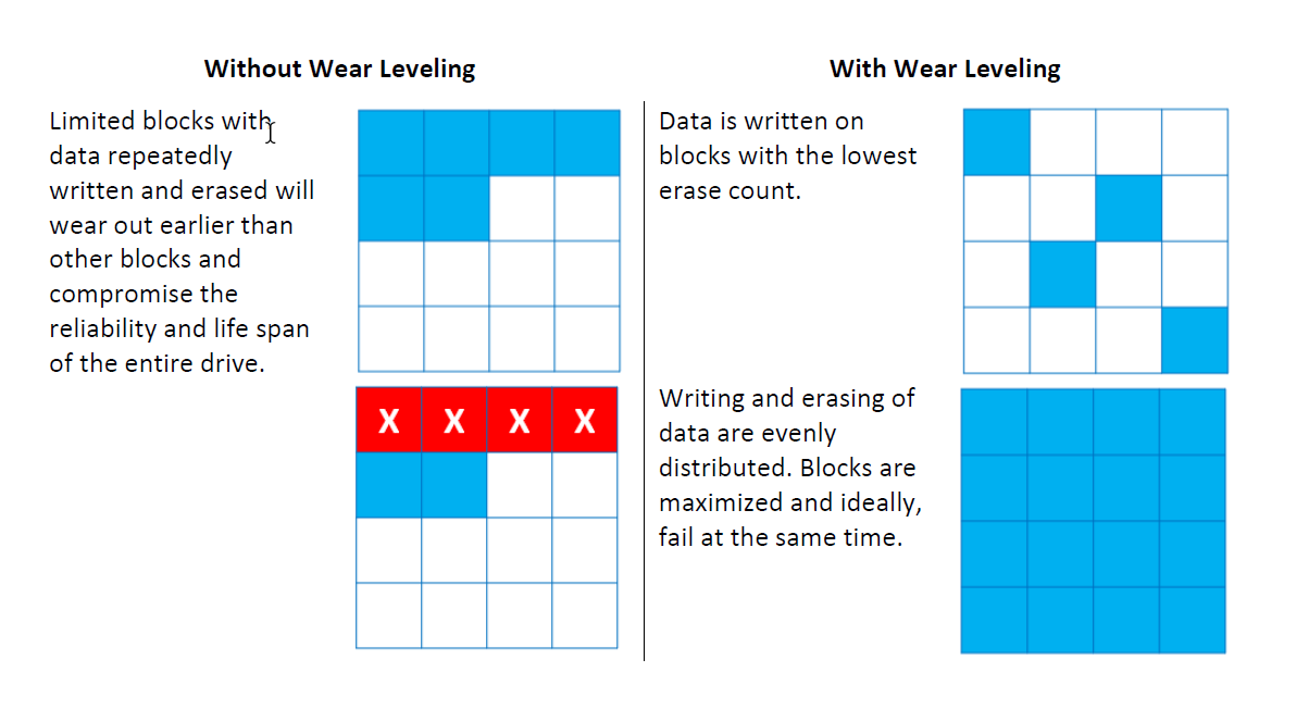
There are three types of wear leveling.
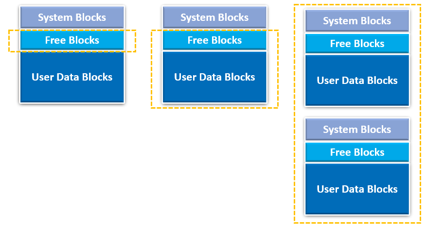
- Dynamic. Makes sure that new data is written only to free blocks with the lowest erase count. The downside is that wear leveling is limited only to "hot" or frequently modified areas, so blocks that hold rarely accessed, static data are not included in the pool of free space, thus limiting the number of blocks going through wear leveling.
- Static. Includes static data or "cold" blocks in the wear leveling process. If a block contains static or rarely accessed data, its write/erase count is low. The data is moved from "cold" blocks to "hot" blocks and the freed-up block is added to the pool of free space for future use. Reassigning static data is a more complex process because it involves multiple operations to move static data around. While more effective at extending flash storage life span, static wear leveling typically covers only a single flash die.
- Global. Works like static wear leveling by including both free space and blocks with static data, but the main difference is that its coverage extends to the entire flash storage device.
The following table and figure illustrate the differences in executed areas:
| Dimension | Dynamic Wear Leveling | Static Wear Leveling | Global Wear Leveling |
|---|---|---|---|
| Die coverage | Single die | Single die | Multiple dies, entire device |
| Blocks leveled | Free blocks only | Free blocks + user data blocks | Free blocks + user data blocks |
ATP Enhanced Wear Leveling
ATP implements global wear leveling on its flash memory products, using an advanced algorithm that carries out both dynamic and static wear leveling to ensure that the flash product is used to the fullest extent of its life span.
ATP Enhanced Wear Leveling treats and manages all NAND flash components in ONE drive as a unified memory management unit. The wear leveling is carried out by the flash controller and is independent of the host system, thus minimizing impact on system performance.
How it works:
There are four main steps for the "enhanced wear leveling" mechanism:
- Establish and update the link table, which is used to convert the host's logical address to the flash memory's physical address.
- Record the "erase counts" of all the blocks in one zone and save them to the wear leveling table. The table is maintained by a RAM register unit in the controller. The table will keep every block's "erase count" within the flash memory ICs.
- Find the static block — a block holding rarely modified data, whose erase count is therefore low — and save its address in the wear leveling pointer. The pointer is used to select the next block to be swapped.
- Check the erase count whenever a block is taken out from the spare pool. If the block's erase count is already higher than the Wear Count Register threshold, it is flagged as "over-count" and should be swapped as soon as possible: the controller swaps it with the static block identified by the wear leveling pointer.
What Wear Leveling Means for Rated Endurance: Industrial SSDs and microSD Cards
The mechanism above is the same across ATP's managed-NAND products — SSDs, SD and microSD cards, and e.MMC — but its effect shows up differently depending on the device. The two questions engineers ask most often:
How does wear leveling improve industrial SSD endurance?
Wear leveling improves industrial SSD endurance by keeping the gap between the most-worn and least-worn blocks small, so the drive's rated endurance reflects the P/E-cycle budget of all its NAND rather than of its busiest blocks. Without it, a workload that repeatedly updates the same logical addresses — databases, logs, metadata — would burn out a small set of physical blocks and push the drive to end-of-life with most of its flash barely used. An endurance rating in terabytes written (TBW) or drive writes per day (DWPD) silently assumes this even spending of cycles; wear leveling is the mechanism that makes the assumption true. Because an SSD contains many NAND dies across multiple channels, coverage matters: ATP applies global wear leveling that manages every die in the drive as one unified pool, which is how its industrial 2.5" SATA SSDs sustain sequential-rated endurance up to 20,480 TB written in 3D TLC and up to 59,250 TB configured in pSLC mode. Under a randomized enterprise workload the same line is rated at 1 drive write per day (DWPD) for 5 years — and the distance between those two figures is exactly why workload type matters when sizing endurance. Two honest boundaries: static wear leveling costs some background data movement (a small write-amplification overhead the algorithm must keep well below the endurance it recovers), and no rating substitutes for measurement — size against your actual write pattern and track wear through the drive's S.M.A.R.T. attributes rather than assuming the datasheet ceiling.
How does wear leveling extend industrial microSD card lifespan?
Wear leveling extends industrial microSD card lifespan by spreading P/E cycles across every block in the card — and in a card, that protection is proportionally more important than in an SSD. A microSD card packs its NAND into a single tiny package with far fewer dies and much less spare area than an SSD, and its typical workloads are pathologically uneven: a FAT/exFAT file system rewrites the same file-allocation-table sectors on nearly every write, and surveillance or dashcam loop recording continuously updates a small set of directory and metadata blocks. Without wear leveling, those few physical blocks absorb thousands of cycles while the rest of the card sits idle, and the card fails at a fraction of its potential life. ATP's industrial microSD cards counter this with the same advanced wear leveling used in its SSDs, executed by the card's own controller and invisible to the host: hot logical addresses are remapped across all physical blocks, and rarely changed data is periodically relocated so even "cold" blocks contribute their cycles. That is what supports card-level ratings up to 5,500 TB written in 3D TLC and up to 12,670 TB in pSLC mode — figures rated under sequential writes, so continuous random-write duty should be sized with margin. Worth stating plainly: consumer cards also perform some wear leveling, but it is often dynamic-only and never published as an endurance rating you can design against. The industrial difference is full static-plus-global coverage, a published TBW, and — on ATP cards — SD Life Monitor to read out remaining life so replacement is planned, not discovered.
The same honest exception applies to both: if a device writes rarely — a boot drive, a configuration store, a mostly-read reference image — wear leveling has little work to do, and paying for pSLC-class endurance buys headroom that will never be used. Match the endurance grade to the measured write load; wear leveling then ensures none of what you paid for is wasted.
Conclusion
Wear leveling is needed to address the finite program/erase capability of NAND flash memory cells. When only a limited number of blocks are repeatedly used, the device can prematurely wear out. By evenly distributing the program/erase cycles over the entire flash storage device, the ATP Enhanced Wear Leveling mechanism makes sure that all memory cells are used to the maximum, thereby extending the life span of the device.
For more information on ATP's wear leveling techniques and other technologies that extend the life expectancy of its "Industrial Only" flash storage products, visit the ATP website or contact an ATP Representative.
Frequently Asked Questions (FAQ)
Q1: How does wear leveling extend industrial microSD card lifespan?
A: Wear leveling extends industrial microSD card lifespan by distributing program/erase (P/E) cycles evenly across all NAND blocks in the card, preventing write hot spots — file allocation tables, loop-recording metadata — from exhausting a few blocks while the rest sit idle. This matters more in a card than in an SSD because a microSD card has far fewer NAND dies and much less spare area to absorb uneven wear. ATP industrial microSD cards run advanced wear leveling in the card controller, independent of the host, supporting endurance ratings up to 5,500 TB written in 3D TLC and up to 12,670 TB in pSLC mode; because those figures are rated under sequential writes, continuous random-write applications should be sized with margin.
Q2: How does wear leveling improve industrial SSD endurance?
A: Wear leveling improves industrial SSD endurance by ensuring the drive's TBW or DWPD rating draws on the P/E cycles of every NAND block, not just the frequently written ones — without it, hot data would wear out a small set of blocks and end the drive's life with most of its flash unused. ATP applies global wear leveling that manages all NAND dies in the drive as one pool, supporting ratings up to 20,480 TB written in 3D TLC and 59,250 TB in pSLC mode on its industrial 2.5" SATA SSDs (rated separately at 1 drive write per day for 5 years under enterprise random workload). Wear leveling does not add endurance beyond what the NAND provides; it prevents that endurance from being wasted.
Q3: What is the difference between dynamic, static, and global wear leveling?
A: Dynamic wear leveling levels wear only across free blocks — each new write goes to the free block with the lowest erase count, but blocks holding unchanged data never rotate into the pool. Static wear leveling adds those "cold" blocks: rarely modified data is periodically moved so low-wear blocks are freed for new writes, extending coverage to the whole die at the cost of some background data movement. Global wear leveling applies the same policy across every NAND die in the device, treating all flash in one drive or card as a single wear pool. Coverage — and endurance benefit — increases in that order; ATP Enhanced Wear Leveling combines all three.
Q4: Does wear leveling eliminate SSD or memory card wear-out?
A: No. NAND flash cells still tolerate only a finite number of P/E cycles, and wear leveling cannot raise that limit — it ensures the device reaches its full rated endurance instead of failing early from uneven wear. A workload that exceeds the device's TBW rating will wear the device out regardless of the algorithm; the remedy is flash with more cycles per cell (pSLC or SLC), higher capacity to spread the same writes over more blocks, or reducing the write load. Wear leveling determines whether you get the endurance you paid for, not how much endurance exists.
Q5: How can I check how much life is left in an industrial SSD or microSD card?
A: Industrial SSDs report wear through S.M.A.R.T. attributes — average/maximum erase counts, percentage of life used, and total bytes written — which the host can poll to plan replacement before end-of-life. For memory cards, ATP provides SD Life Monitor, which reads remaining life directly from the card so surveillance recorders, gateways, and vehicle systems can schedule swaps during maintenance windows instead of discovering a worn-out card after data loss. Comparing reported wear against the device's rated TBW converts the datasheet figure into a concrete remaining-life estimate for your actual workload.