While hard disk drives (HDDs) and solid state drives (SSDs) both store data, the way they work is vastly different. One of their key differences is in how they write and erase data to make more memory space available.
When a user deletes a file, for example, the operating system (OS) will simply mark the deleted file. The next time another write is performed, the HDD will write the new file over any available space and even overwrite the space where the marked deleted file was stored.
The process is different on a NAND flash storage device. Data is stored in integrated chips (ICs) that are organized into pages, and several pages make up a block. Writing (programming) is done on a page level but erasing is done on a block level.
The following illustration shows the layout of a NAND flash memory chip -- A physical NAND page is a group of NAND flash cells belonging to the same block. A NAND block is composed of several pages. Several NAND blocks form a plane. Finally, planes form a die. Each memory chip contains one or more dies.
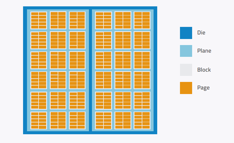
Figure 1. NAND flash layout
Garbage Collection
Garbage collection is an important function of the NAND flash controller. The goal is to enable the flash storage device to have enough spare blocks so that whenever data must be written, the device does not have to wait for a block to be erased and made available for the new data.
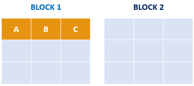
The following steps show how garbage collection is done.
Pages A, B & C in Block 1 contain active data.
The remaining pages in the block are free and available whenever
new data needs to be written or stored.
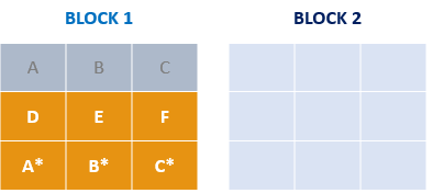
Data in pages A, B and C in Block 1 have been modified and replaced as A*, B* and C*.
New data have been written to pages D, E and F.
Pages A, B and C are now marked as invalid or stale; however,
they cannot be written with new data unless the entire Block 1 is erased.
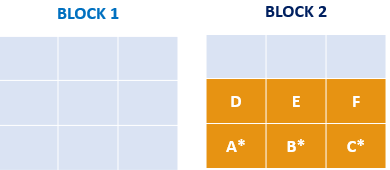
Garbage collection is performed.
Valid data in pages D, E & F as well as A*, B* & C* are copied to spare Block 2.
All pages in Block 1 are erased and the block is now available
to be written with new data. (Reference: ExtremeTech)
TRIM & Deallocation Commands
Flash storage devices typically cannot detect which pages contain data marked for deletion, causing them to erase and rewrite entire blocks during the garbage collection process. This results in blocks keeping invalid data for a long time instead of being erased sooner to be used for new writes. As more files are written on the flash storage device and there are fewer spare blocks to move data into, the device will have to wait for blocks to be erased before it can accept new data. This causes performance bottlenecks and the device slows down.
The TRIM command is an Advanced Technology Attachment (ATA) command available for flash storage devices using the Serial ATA (SATA) interface. For NVMe modules using the PCIe interface, the equivalent command is “Deallocate.” TRIM and Deallocate complement garbage collection by notifying the flash storage device ahead of time which specific pages in a block may already be erased. The pages with invalid data are marked for deletion, valid data are moved to a free block, and the device is “permitted” to erase the block containing invalid data any time. This allows more blocks to be available for new data to be written in, and the storage device performs faster.
ATP’s Efficient Storage Space Reclamation
ATP flash storage devices perform background garbage collection to clean up the drive without slowing down write performance. They also support the TRIM and Deallocate commands to optimize performance and improve endurance. Used in applications where devices are expected to operate for extended stretches of time in harsh conditions, ATP’s “Industrial Only” memory and storage solutions are built for high performance and long endurance to deliver the best total cost of ownership (TCO) value.
For more information about technologies supported on ATP products, visit the ATP website or contact an ATP Representative or Distributor in your area.