The amount of data being generated every day is growing exponentially. According to Exploding Topics, approximately 402.74 million terabytes of data are created daily and around 181 zettabytes will be generated this year, with videos accounting for over half of Internet data traffic.
In this primer, we explore the different types NAND die packages, the challenges that come with expanding capacities and NAND die stacking, and ATP’s groundbreaking solution to overcome these challenges.
NAND Die Packages:
Their Critical Role in Defining NAND Flash Architecture
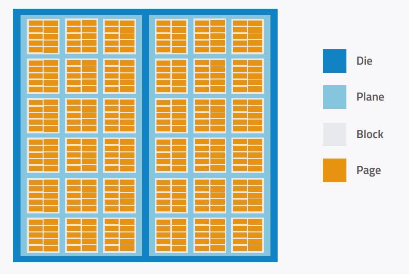
A basic NAND flash layout is shown below, where several pages form a block. Several blocks form a plane. Planes form a die, and one or more dies form a memory chip. A NAND die package is an integrated circuit (IC) package that contains one or more NAND flash memory dies.
NAND die packages vary in complexity. The following table shows the different types and their typical use cases.
| Package Type | Number of Dies per Package | Typical Use Case |
|---|---|---|
| Single Die Package (SDP) | 1 | Low-capacity storage for cost-sensitive applications where space and power are minimal concerns. |
| Double Die Package (DDP) | 2 | Moderate-capacity storage, offering higher density without significantly increasing package size. Ideal for mid-tier industrial storage. |
| Quad Die Package (QDP) | 4 | Higher-capacity storage commonly used in mainstream solid state drives (SSDs). |
| Octal Die Package (ODP) | 8 | High-capacity storage used in SSDs where space savings and performance are key. |
| Hexadeca Die Package (HDP) | 16 | Very high-capacity storage supporting enterprise SSDs that require minimal printed circuit board (PCB) footprint while maximizing density. |
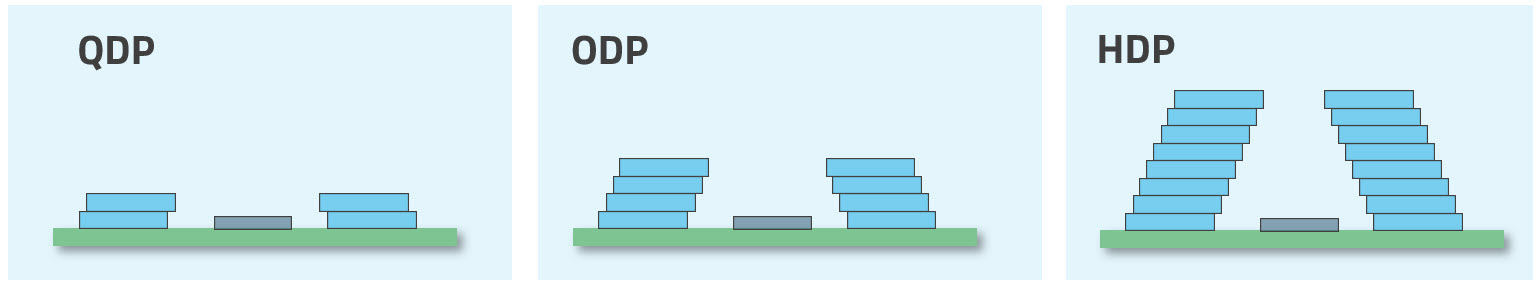
illustration of Quad Die Package (QDP), Octal Die Package (ODP) and Hexadeca Die Package (HDP)
Why Use NAND Die Packages?
The surge in the demand for higher capacities in server/data centers is largely driven by the explosive growth in artificial intelligence (AI) workloads. These workloads require massive computational resources and data storage. With real-time AI processing offering reduced latency and faster data analytics, Edge AI’s need for more storage is also fueling the growth of edge data centers.
The continued increase in data generation requires not only higher capacities in centralized and distributed data centers but also miniaturization. Devices such as wearables, sensors, and embedded systems are getting smaller, in turn also requiring more storage for less footprint, which leads to die stacking.
- Higher Capacity: Large amounts of data can be stored within a small footprint, especially when multiple dies are stacked.
- Space Efficiency: Vertical stacking allows fewer die packages on a printed circuit board (PCB), thus saving space and potentially lowering manufacturing costs.
- Performance Boost: Multiple-die packaging allows parallelism (parallel data access), so data can be read/written simultaneously for enhanced performance.
Each type of NAND die package offers distinct advantages. Choosing the right configuration requires careful consideration of the density, performance, cost, and design complexity, as well as possible tradeoffs like advanced thermal requirements and power management design.
What is the Relationship Between the SSD Controller and NAND Die Package Configuration?
While vertical die stacking allows capacity expansion and performance enhancements, it may also impact timing and signal management. It is the SSD controller’s job to manage and ensure the effectiveness of the NAND die package configuration.
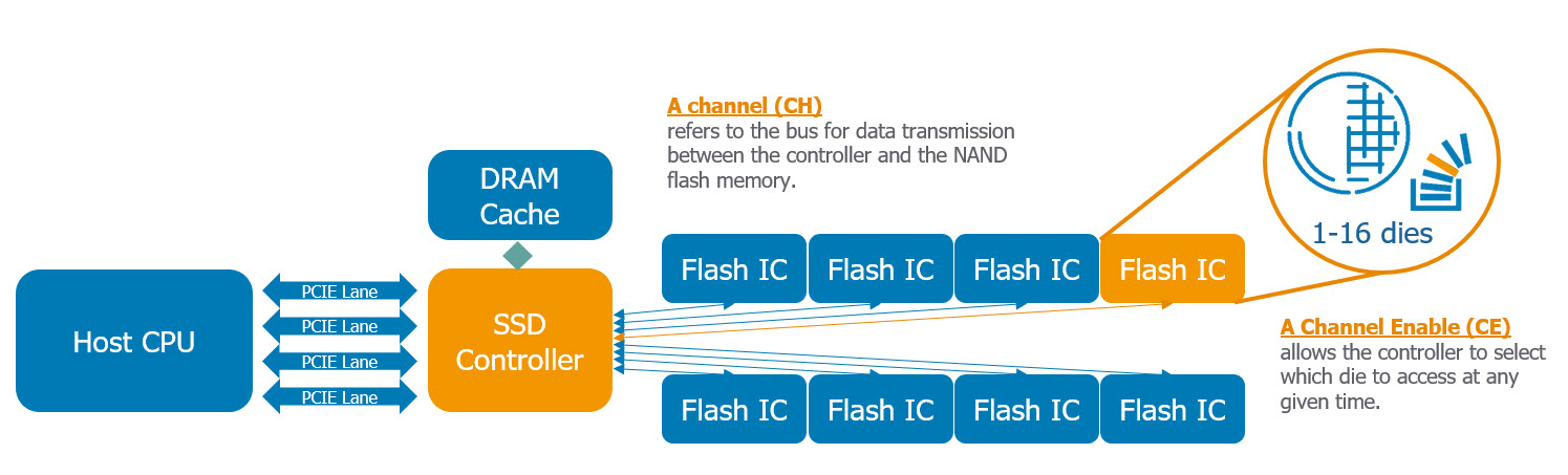
A channel (CH) refers to the bus for data transmission between the controller and the NAND flash memory. The controller communicates with one or more dies simultaneously through the channels. With more channels, more data can be transmitted simultaneously. Greater parallelism, or parallel data access, enables faster speeds and boosts performance.
A Channel Enable (CE) allows the controller to select which die to access at any given time. The die responds to the controller’s requests when CE is activated, while the others remain inactive. This ensures that the controller can effectively manage multiple dies on the same channel without interference.
The following table shows how many 1 Tb dies are needed in a 16 TB and 8 TB drive, and how the controller configuration manages these dies.
| Controller Configuration | Dies per CE | Total Dies | Capacity per Die | Total Capacity |
|---|---|---|---|---|
| 8 CH x 8 CE = 64 CE | 2 | 64 CE x 2 dies = 128 | 1 Tb = 128 GB | 16 TB: 128 dies x 128 GB |
| 8 CH x 4 CE = 32 CE | 4 | 32 CE x 4 dies = 128 | 1 Tb = 128 GB | 16 TB: 128 dies x 128 GB |
| 4 CH x 4 CE = 16 CE | 4 | 16 CE x 4 dies = 64 | 1 Tb = 128 GB | 8 TB: 64 dies x 128 GB |
Tb: Terabit , TB: Terabyte, GB: Gigabyte
What are the Challenges of Higher-Density NAND Die Packaging?
Voltage and electrical problems become more difficult to manage as NAND packages get more complicated with more stacking and higher density. These are some of the crucial challenges faced by NAND flash storage manufacturers as they attempt to balance higher capacities with reliability, power efficiency, and signal integrity.
- Voltage requirements increase as die stacking increases. This leads to greater susceptibility and signal degradation.
- Heat dissipation becomes critical as dies are packed in limited spaces.
- Signal integrity issues arise due to longer internal paths and complex interconnects.
- Power efficiency and reliability become more difficult to maintain as operating stress also increases.
How Does AcuCurrent Technology Solve These Issues Across Temperature Variations and Extremes?
ATP AcuCurrent addresses signal integrity challenges proactively to ensure that even higher-density, higher-stack NAND configurations (with die packages like QDP/ODP/HDP) can operate smoothly in any environment.
Dynamic Current Adjustment in Real Time
In contrast to static signal configurations, AcuCurrent dynamically adapts to temperature variations to optimize signal integrity. It continuously tunes drive settings in real time to respond to temperature changes, ensuring stable signal transmission in different operating conditions. This technology maintains consistent performance and prevents failures (such as cold boot issues or heat-induced slowdowns) in harsh industrial settings, extending SSD lifespan and improving overall system dependability.
Reduced Read Retries and Lower Error Rates
More NAND dies stacked into a package can lead to signal degradation due to longer trace lengths. This also makes SSDs susceptible to Read Retry events caused by crosstalk or interference. By optimizing signal integrity in multi-die NAND packages, AcuCurrent significantly reduces the need for read-retry cycles and lowers raw bit error rates, leading to cleaner and more reliable signal transmission as well as faster data access.
| Driving Setting* | SSD #1 Read Retry Count @70C | SSD #2 Read Retry Count @70C | SSD #3 Read Retry Count @70C | SSD #4 Read Retry Count @70C |
|---|---|---|---|---|
| Fixed setting | 240 | 6 | 622 | 687 |
| Dynamic setting | 0 | 0 | 0 | 0 |
Adaptive Current Adjustments and Enhanced Power Efficiency
Different NAND configurations exhibit diverse behaviors in terms of current draw and response times that fixed settings cannot address. AcuCurrent dynamically adjusts driving strength and timing, thus reducing unnecessary power draw, preventing excessive signal compensation, and improving power efficiency.
Wide Temp Resilience
Improved reliability and stable performance across wide temperature ranges up to 125℃ (-40℃ to 85℃) ensures high data integrity as SSDs move to higher capacities and more complex stacking. This mitigates risks of data loss or corruption that can arise from signal integrity issues inherent in dense or multi-die package environments.
Versatile Support for a Wide Range of NAND Configurations
Mix-die stack packages are used in NAND flash storage devices depending on market demand, cost, and availability. AcuCurrent automatically adapts, allowing ATP SSDs to maintain consistent reliability regardless of die package used.
Conclusion
The rate of data generation continues to expand exponentially, driving the evolution of NAND flash technologies to enable high-capacity storage within limited footprints.
Different NAND die package configurations allow capacity expansion, with each type of package offering distinct advantages. As SSDs are configured to meet diverse and complex data storage requirements, they also face numerous challenges that come with the persistent demand for higher capacities. Among these challenges is signal degradation arising from increased NAND die stacking.
ATP AcuCurrent technology directly addresses the signal integrity and reliability challenges posed by increasing SSD capacities and diverse NAND die packages.
By employing real-time, dynamic signal optimization at both the firmware and hardware levels, AcuCurrent ensures robust performance, low latency, and high data integrity across a wide range of SSD configurations and operating environments.
For more information on ATP AcuCurrent and NAND flash storage solutions in different die package configurations, contact an ATP Distributor/Representative in your area or visit the ATP website.