e.MMC Primer
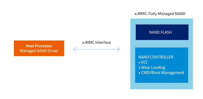
Embedded MultiMedia Controller, or e.MMC, is an advanced managed NAND flash storage solution soldered directly to the motherboard. It integrates the following components in the same IC package:
- MMC interface
- NAND flash memory
- NAND flash controller
In contrast to "raw" NAND solutions like typical solid state drives (SSDs) or SSD modules that require an external hardware controller, e.MMC is "managed" NAND – it combines raw NAND and a sophisticated controller in an integrated package so memory management is done internally.
-
Internal NAND management frees the host from having to perform low-level flash background operations such as wear leveling, bad block management, error correction and other functions.
-
Simplified qualification process reduces time-to-market.
-
High throughput support for large data transfers deliver the performance required by mobile devices.
-
Low power consumption makes the e.MMC a cost-effective solution for space-constrained systems.
-
Simplified memory interface design allows e.MMC to be extremely compact and provides support for future flash storage devices. It is smaller than a postage stamp, making it suitable for automotive and industrial applications requiring rugged endurance, reliability and durability in challenging operating environments.
-
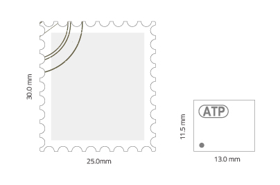
Figure 2. Size comparison between a postage stamp and an e.MMC card.
Usage
e.MMC is a universal data storage and communication media and is typically used in portable applications. Its small footprint makes it a preferred choice for mobile devices such as smartphones, tablets and laptops. Increasingly, e.MMC is also gaining wide acceptance in embedded systems for industrial and automotive applications, such as infotainment systems, aerospace/avionics, Internet of Things (IoT), industrial automation, and other applications.
Latest Standard
JEDEC published the latest version of the e.MMC standard in February 2015. JESD84-B51: Embedded MultiMediaCard (e.MMC), Electrical Standard (5.1), also known as e.MMC v5.1, defines new features and updates. The table below shows a comparison of features available on recent e.MMC versions.
|
Features |
Version / Year |
||
|
4.51 (2012) |
5.0 (2013) |
5.1 (2015) |
|
|
Max. Bus Speed Mode |
HS200 |
HS400 |
|
|
Max. Data Transfer |
200 MB/s |
400 MB/s |
|
|
Max. Clock Frequency |
200 MHz SDR |
200 MHz DDR |
|
|
Command Queuing |
- |
ü |
|
|
Cache Barrier |
- |
ü |
|
|
Enhanced Data Strobe |
- |
ü |
|
|
Cache Flushing Report |
- |
ü |
|
|
Secure Write Protection |
- |
ü |
|
|
Data Strobe |
- |
ü |
|
|
Data Bus Width* |
4/8 bits |
8 bits |
|
|
Production State Awareness |
- |
ü |
|
|
Field Firmware Update |
- |
ü |
|
|
Device Health Report |
- |
ü |
|
Table 1. Specifications comparison of different e.MMC versions.
*Versions 4.51/5.0/5.1 support all data bus widths (1/4/8 bits) when providing backward compatibility for lower speeds such as those of legacy MMC cards, high-speed SDR and high-speed DDR.
Version Change Highlights
|
v4.51 to v5.0 |
v.5.0 to v5.1 |
|---|---|
|
HS400 Mode introduced to enhance sequential read/write performance from 200 MB to 400 MB. |
Command Queuing and Cache Barrier added to enhance random read/write performance. |
|
Production State Awareness (PSA) introduced to secure pre-load data during the e.MMC/PCB soldering process. |
Cache Flushing Report added to ensure the data integrity on cache blocks. |
|
Field Firmware Update (FFU) introduced to allow features enhancement in the field by updating the e.MMC firmware that is fixed on a PCB. |
Enhanced Strobe in HS400 Mode added to facilitate faster synchronization between the host and the e.MMC device. |
|
Device Health Report introduced to monitor the health condition of an e.MMC. |
Secure Write Protection added to ensure that only trusted entities can protect or unprotect the e.MMC device. |
e.MMC v5.1 Performance
According to the JESD84-B51 standard, e.MMC v5.1 supports the following bus speed modes and clock frequencies.
|
Mode Name |
Data |
I/O Voltage |
Bus Width |
Frequency |
Max. Data Transfer (MB/s, implies x8 |
|
HS400 |
Dual |
1.8/1.2 V |
8 |
0-200 MHz |
400 MB/s |
|
HS200 |
Single |
1.8/1.2 V |
4, 8 |
0-200 MHz |
200 MB/s |
|
High-Speed DDR |
Dual |
3/1.8/1.2 V |
4, 8 |
0-52 MHz |
104 MB/s |
|
High-Speed SDR |
Single |
3/1.8/1.2 V |
1, 4, 8 |
0-52 MHz |
52 MB/s |
|
Backward Compatibility |
Single |
3/1.8/1.2 V |
1, 4, 8 |
0-26 MHz |
26 MB/s |
Table 2. e.MMC 5.1 bus speed modes and clock frequencies.
Comparison with Other NAND Flash Storage Products
How is e.MMC different from other NAND flash storage products such as solid state drives (SSD), memory cards and universal flash storage (UFS)? Although storage products all use NAND flash memory chips, they are different in many ways aside from their physical appearance.
Information on this table is based on ATP product specifications.
|
Feature |
NAND Flash Product |
|||||
|---|---|---|---|---|---|---|
|
e.MMC |
Memory Cards |
UFS** |
SSD |
|||
|
Protocol |
MMC |
SD |
SCSI |
AHCI (SATA); NVMe |
||
|
Interface |
HS400 |
UHS-I/UHS-II* |
Serial Interface |
SATA; PCIe |
||
|
Form Factor(s) |
153-pin FBGA embedded |
SD/microSD |
Card (removable); BGA (embedded) |
2.5" drives; M.2; eSATA; SlimSATA; mSATA, eUSB |
||
|
NAND Flash Type |
Managed |
Managed |
Managed |
Raw |
||
|
Data Transfer Speed (Max.) |
400 MB/s |
UHS-1: 104 MB/s |
2-lane gear 2: 2-lane gear 3: |
SATA: 550 MB/s PCIe: 32 Gb/s |
||
|
Dimensions |
11.5 x 13 x 1.3 |
SD |
32 x 24 x 2.1 |
11.5 x 13 x 1.0 |
2.5" SSD |
100.0 x 69.9 x 9.2 |
|
microSD |
15 x 11 x 1.0 |
M.2 2242 |
42 x 22 x 3.5 |
|||
|
M.2 2260 |
60 x 22 x 3.5 |
|||||
|
M.2 2280 |
80 x 22 x 3.5 |
|||||
|
SlimSATA |
54 x 39 x 4 |
|||||
|
mSATA |
50.8 x 29.85 x 3.4 |
|||||
|
eUSB |
36.9 x 26.6 x 9.5 |
|||||
Table 3. Key differences of e.MMC from other NAND flash storage products.
*Ultra High Speed bus interface
**UFS availability TBA.
Size Comparison
The figure below shows the different sizes of ATP flash storage products along with the e.MMC.
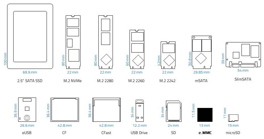
Figure 4. ATP e.MMC size compared with other ATP NAND flash storage products
ATP industrial/automotive-grade e.MMC comes in a 153-ball Fine Pitch Ball Grid Array (FBGA) and is designed to meet high-performance data transfer, code and data storage requirements as well as automotive applications such as in-vehicle infotainment. Constructed using 3D MLC NAND flash memory, the ATP e.MMC achieves higher densities with up to 128 GB of memory for use as mass storage.
The ATP e.MMC complies with JEDEC e.MMC standard v5.1 and is backward compatible with other e.MMC versions (v4.41/v4.5/v5.0). It supports features such as power-off notifications, packed commands, cache, boot or replay protected memory block (RPMB) partitions, high priority interrupt (HPI), and hardware (HW) reset.
ATP e.MMC Solutions
|
Product |
e.MMC |
||
|---|---|---|---|
|
Product Line |
Premium |
Superior |
|
|
Naming |
E700Pi |
E600Si |
|
|
IC Package |
153-ball FBGA |
||
|
JEDEC Specification |
v5.1, HS400 |
||
|
Flash Type |
3D SLC Mode |
3D NAND |
|
|
Density* |
8 GB to 64 GB |
16 GB to 128 GB |
|
|
Bus Speed Modes |
x1/x4/x8 |
x1/x4/x8 |
|
|
Performance** |
Sequential Read/Write |
300/220 |
300/220 |
|
Random Read/Write |
15K / 30K |
15K / 30K |
|
|
Operating Temperature |
-40°C to 85°C (industrial) |
||
|
Reliability |
Max. TBW** |
651 TB |
372 TB |
|
MTBF @ 25°C |
> 2,000,000 Device hours |
> 2,000,000 Device hours |
|
|
VCC (Typical RMS in Read/Write) |
130 / 215 |
130 / 215 |
|
|
VCCQ (Typical RMS in Read/Write) |
115 / 105 |
115 / 105 |
|
|
L x W x H (mm) |
11.5 x 13.0 x 1.3 (max.) |
||
Table 4. ATP industrial e.MMC specifications
* 1 GB=1,000,000,000 bytes. Actual user storage may be less.
**Based on internal testing; performance may vary depending upon drive capacity, file attributes, host device, OS and application. Cache On.
e.MMC is a cost-effective, reliable embedded mass storage device that integrates the NAND flash memory, controller and interface in one package. ATP's e.MMC solutions offer reliable storage for applications requiring high performance and endurance as well as low power consumption.
Please visit the ATP e.MMC product page or contact an ATP Representative or Distributor in your area for more information.