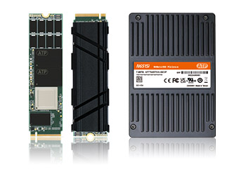
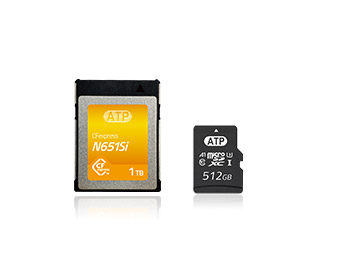
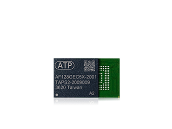
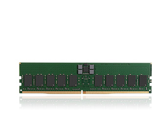
Industrial SSDs, SD NAND Flash products and DRAM Modules
Höchste Zuverlässigkeit und Langlebigkeit für anspruchsvollste industrielle Anwendungen
Networking / Telekom
hohe Datenströme, ständige Erreichbarkeit und unterschiedliche Zugriffsprofile in einem Telekommunikationssystem benötigen schnelle & zuverlässige Speichermedien mit hohen Kapazitäten
Erfahren Sie mehrSpeicherlösungen für Automotive
Automotive Anwendungen benötigen robuste Bauteile die auch unter schwierigen Bedingungen zuverlässig arbeiten und sicheres, komfortables Fahren ermöglichen
Erfahren Sie mehrDefense / Aerospace
ATP Electronics bietet eine breite Palette an robusten Lösungen für große Temperaturbereiche, ohne hohe Mindestbestellmengen (MOQ), mit langjähriger Verfügbarkeit und der Möglichkeit vielfältiger Anpassungen für spezielle Anwendungsbereiche.
Erfahren Sie mehrIndustrial / Automation
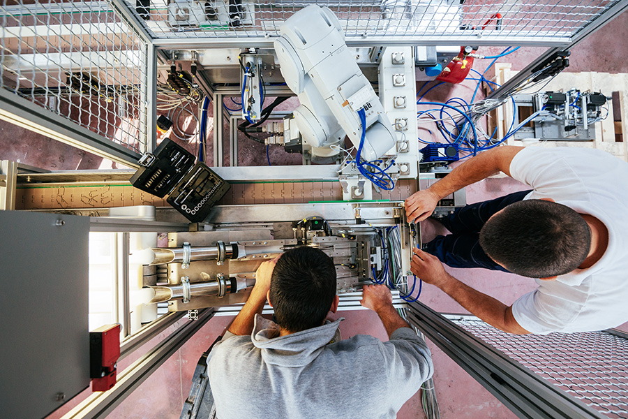
ATP offers a full spectrum of legacy and latest-generation memory and NAND flash storage solutions in a variety of form factors that meet the stringent requirements of industrial and automation systems
Erfahren Sie mehrTransportation
For public transportation systems, our fundamental competitiveness in endurance, longevity, wide-temp, fix BOM control, and delivers suitable industrial storage and memory solutions.
Erfahren Sie mehr- Networking / Telekom
- Speicherlösungen für Automotive
- Defense / Aerospace
- Industrial / Automation
- Transportation
Aktuelle Neuigkeiten

Veranstaltungskalender
Computex 2026
R0914
ATP Electronics,showcases its Specialized Storage & Memory Solutions at Taipei Nangang Exhibition Center, Hall 2, 4F — Booth R0914
Alle Veranstaltungen
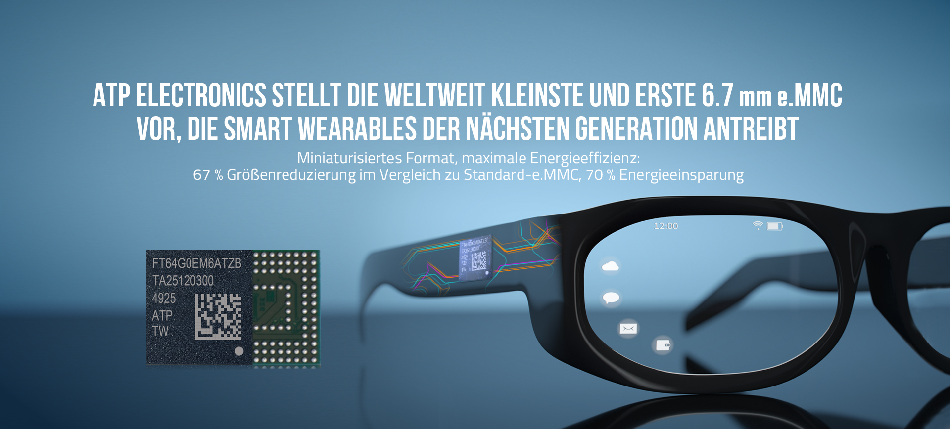
ATP Electronics at Embedded World 2026: Redefining Wearable Storage, Endurance, Memory Reliability
ATP Electronics will debut the World’s Smallest 6.7 mm e.MMC at Embedded World 2026.

ATP Anzcham Charity Bike Ride
After 5 incredible days and 538 km 🚴♂️🚴♂️🚴♂️, ATP Representatives and fellow participants crossed the finish line in Tainan today!

What Procurement Teams Need to Know Before Buying Industrial SSDs
Discover how engineers and procurement teams can align on industrial SSD selection to ensure reliability, longevity, and lower total cost of ownership.

Memory Wars: Why HBM Is the Hottest Commodity in AI
CONNECTED presenter Susan Chow engages in an insightful conversation with ATP Electronics President and CEO Jeffray Hsieh at COMPUTEX/InnoVEX 2025.


ATP Electronics Publishes Its First Sustainability Report, Marking a Corporate Responsibility Milestone
ATP supports mission-critical systems with reliability at the core—driving our commitment to sustainability and our first Sustainability Report.
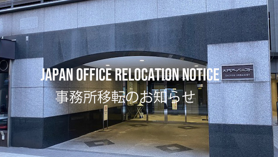
Mehr ErfahrenJapan Office Relocation Notice
ATP Electronics Japan, Ltd., are pleased to announce that our office will be relocating to a new address.
Mehr ErfahrenATP Electronics: Committed to a PFAS-Free Future for Your Safety and the Environment
At ATP Electronics, we are committed to the safety and well-being of our customers and the environment. We understand the growing concern regarding Per- and polyfluorinated alkyl substances, or PFAS, and their widespread use in consumer products. These pe
Mehr ErfahrenSmart Factories: The Color of the Future is Green
As a true manufacturer, ATP Electronics recognizes that smart manufacturing is a leading driver of ESG. Policies on the environment and sustainability continue to increase in importance amid critical concerns such as climate change.
Mehr ErfahrenATP Electronics Shows Support for Vulnerable Children,Joins Chung Yi Social Welfare Foundation Fundraiser to Build New Orphanage
The charity event, “Putting Effort Into Love Homes,” was aimed to promote awareness of Chung Yi Social Welfare Foundation’s advocacy to provide warm homes and professional services for vulnerable children and to raise funds for building new orphanages.
Mehr ErfahrenATP Electronics Spreads the Warmth of Love and Sharing at NCCU Auction Banquet
ATP was privileged to have had the opportunity to participate in a charity auction that aimed to benefit two humanitarian foundations for people with special needs.
Mehr ErfahrenWinning the Flash Memory and Storage Circuit: Lessons from the Racetrack
The industrial and embedded segment may be likened to motorsports racing, where choosing the right car and car settings for the right racetrack is critical to winning.
Mehr ErfahrenNVMe SSD Thermal Management: What We Have Learned from Marathons
Marathons and the thermal throttling management of NVMe SSDs have these five things in common, each of which can impact performance
Mehr ErfahrenATP SATA SSDs Qualify for Compatibility and Interoperability with Microchip’s New Tri-Mode Storage Adapters
ATP's A600Sc Series serial ATA solid state drives (SATA SSDs) have been successfully qualified for compatibility and interoperability with Adaptec® Smart Storage PCIe® Gen 4 Tri-Mode SmartRAID 3200, SmartHBA 2200, and HBA 1200 Smart Storage adapters.
Mehr ErfahrenATP is committed to protecting your privacy. To meet the requirements of the new EU General Data Protection Regulation (GDPR), we have updated our Privacy Policy to let you know how we collect data to deliver enhanced content and experience on the ATP site.

