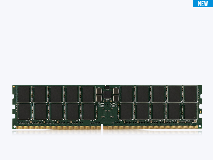
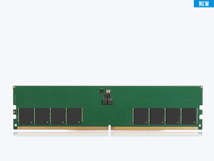
DDR5 has two different kinds of ECC that are easy to confuse. On-die ECC, built into every DDR5 chip, corrects single-bit errors inside the chip; side-band (DIMM-wide) ECC, the kind servers have always used, protects data across the whole link to the CPU. On-die ECC does not make a standard DDR5 module an ECC module.
Key Takeaways
- On-die ECC corrects single-bit errors inside the DRAM chip before data is sent to the CPU. It improves the reliability of individual chips as cells shrink — it is not a replacement for traditional, side-band ECC.
- Side-band (DIMM-wide) ECC protects data in transit across the whole link, from the DRAM chip and module to the memory controller in the CPU. This is the traditional ECC servers have always used, typically SEC-DED: single-error correct, double-error detect.
- Every DDR5 chip includes on-die ECC by JEDEC mandate, allocating 8 bits of ECC storage for every 128 bits of data. It does not turn a standard DDR5 module into a server-grade ECC module.
- ECC modules are wider modules, so they carry more chips. DDR2-DDR4 ECC uses a 72-bit bus (nine x8 chips for 1Rx8); a DDR5 RDIMM uses an 80-bit bus, and registered DIMMs are always side-band ECC.
- On-die ECC and side-band ECC are complementary, not interchangeable. Servers, workstations, and other zero-error environments still require side-band ECC DIMMs even though every DDR5 chip ships with on-die ECC.
- Transportation memory is governed by a stack of standards, not one: AEC-Q100 qualifies the DRAM ICs (Grade 3 covers −40°C to 85°C ambient), ISO 26262 governs functional safety, IATF 16949 governs production quality — and EN 50155 adds railway-specific environmental requirements.
- Medical standards certify the device, not the DRAM inside. IEC 60601-1 and ISO 13485 apply to the end equipment and its manufacturer; memory supports compliance through host-visible error correction, a controlled bill of materials, and long-term supply.
- On-die ECC alone is not enough for safety-critical designs. Where a system must demonstrate error detection — a vehicle controller, a patient monitor — specify side-band ECC modules, which report errors to the host. For non-critical functions such as infotainment or display processing, non-ECC DDR5 with its built-in on-die ECC is often adequate.
Two Kinds of ECC, Easily Confused
As dynamic random access memory (DRAM) capacity grows with each generation and wafer lithography shrinks for higher speeds and better economies of scale, bit errors become more likely. DDR5 answers this on two fronts that are easy to confuse: on-die ECC, built into every chip, and the traditional server-grade ECC DIMM, which adds error correction at the module level.
Both are called ECC (Error Correction Code), but their protection scope, purpose, and mechanism differ. Mistaking one for the other leads to a common wrong conclusion — that a standard DDR5 module is now an ECC module. It is not. This guide explains what each does, why DDR5 mandates on-die ECC, the chip-count math behind ECC modules, and whether you still need an ECC DIMM.
What is On-Die ECC? Is It the Same as Traditional ECC?
On-die ECC is an error-correction mechanism built into the DDR5 chip that corrects single-bit errors within the DRAM before data is sent to the central processing unit (CPU). It provides additional protection at the chip level, but it is not the same as traditional ECC. Three points clarify what it is and is not:
- It is not a replacement for DIMM-wide or side-band ECC. It is designed to improve the reliability of individual chips, so on-die ECC has more to do with chip reliability and yield than with end-to-end data integrity.
- It exists because denser cells flip more easily. As memory cells become denser, each cell holds less charge, making it more vulnerable to bit flips. On-die ECC manages those bit flips so more cells pass validation during manufacturing and reach JEDEC-required specifications.
- It protects data on the die — not data in transit. It does not protect data moving between the memory module and the CPU or GPU, and cannot correct errors that occur outside the chip, such as on the module traces or at the memory controller.
Why Does DDR5 Feature On-Die ECC?
As the process node advanced to 1-alpha (1a) — the 4th generation of 10-nanometer (nm) technology — chip dimensions shrank, letting DDR5 reach higher speeds and densities. Smaller geometries also raised the likelihood of single-bit errors on the DRAM arrays. The same shrink that creates the problem also frees the die space to carry the fix — DDR5 allocates 8 additional bits of ECC storage for every 128 bits of data.
The mechanism is self-contained. During a write, the DRAM internally computes the ECC code and stores it in that extra space. During a read, it reads back both the data and the code; if it finds a discrepancy, it corrects the single-bit error before outputting data. This is single error correction (SEC) performed entirely inside the chip.
On-die ECC brings three practical benefits:
- Economies of scale: it allows DRAM makers to keep scaling to denser process nodes with acceptable yields by correcting single-bit errors internally. Module manufacturers like ATP build on these higher-density chips to deliver more capacity at lower cost.
- Better data integrity at the chip level: correcting during read commands, before output, reduces the burden on system-level error correction and protects on-die data against single-bit errors in the array.
- Error Check and Scrub (ECS): DDR5 can read internal data and write back corrected data when an error is found, preventing error accumulation in higher-capacity modules. ECS also records DRAM defects and reports error counts to the host for better transparency.
What is Side-Band (DIMM-Wide) ECC?
Side-band ECC, the traditional ECC used in servers and workstations (also called DIMM-wide or module-level ECC), protects data across the entire link: from the DRAM chip, across the module's PCB and the connector, to the memory controller in the CPU. It is the protection on-die ECC explicitly does not provide.
It works end to end. On a write, the CPU's memory controller computes the ECC code before transmitting, and data and code travel together to the module. On a read, the controller reads both back and verifies the whole path — board, socket, and DRAM. Traditional ECC typically detects double-bit errors and corrects single-bit errors (SEC-DED), whether they arise in the stored data or on the path between the controller and the memory — including errors introduced by transmission noise, high-frequency effects, and heat that on-die ECC cannot touch.
On-Die ECC vs Side-Band ECC: The Key Difference
The most fundamental difference is where in the data's journey protection applies. On-die ECC guards data inside the chip; side-band ECC guards the whole link to the CPU.
| Aspect | On-die ECC (baseline DDR5) | Side-band / DIMM-wide ECC (server, workstation) |
|---|---|---|
| Protection scope | Inside the DRAM chip only (cell array to internal buffer) | Full link: DRAM chip, PCB, connector, to the CPU memory controller |
| Primary purpose | Chip reliability and manufacturing yield as cells shrink | End-to-end data integrity in operation; prevents silent corruption |
| Data in transit | Not protected; errors on the path cannot be repaired | Protected; corrects errors introduced on the transmission path |
| Typical capability | Single error correction (SEC) | SEC-DED (correct single-bit, detect double-bit) or stronger |
| Hardware | Built into every DDR5 chip; 8 ECC bits per 128 data bits | Extra ECC bus width and storage on the module |
Table 1. On-die ECC versus side-band ECC — same name, different scope, purpose, and hardware.
Why RDIMMs Are Always Side-Band ECC, and the Chip-Count Math
ECC at the module level is fundamentally about extra bus width, and extra width means extra chips. It is also why registered DIMMs (RDIMMs), built for servers and workstations, are always ECC: the server memory standard assumes error correction.
For DDR2, DDR3, and DDR4, non-ECC modules use a 64-bit data bus and ECC modules use 72 bits. A 1Rx8 ECC module therefore needs 8 data chips plus 1 ECC chip — 9 chips total. DDR5 splits the module into two sub-channels, which changes the arithmetic by form factor:
A 1Rx8 DDR5 ECC UDIMM/SODIMM totals 72 bits, which is 9 chips (72 / 8). A 1Rx8 DDR5 RDIMM totals 80 bits, which is 10 chips. The wider 80-bit RDIMM bus is why it needs the extra chip. This module-level chip count is separate from on-die ECC, which is present on every chip regardless of form factor.
| Module type (1Rx8) | Sub-channel width | Total bus width | x8 chips required |
|---|---|---|---|
| DDR2-DDR4 ECC DIMM | n/a (single 64-bit bus) | 72-bit (64 + 8 ECC) | 9 |
| DDR5 ECC UDIMM / SODIMM | 36-bit (32 + 4 ECC) | 72-bit (2 × 36) | 9 |
| DDR5 RDIMM | 40-bit (32 + 8 ECC) | 80-bit (2 × 40) | 10 |
Table 2. Side-band ECC chip count for a 1Rx8 module, by form factor. DDR5's two-sub-channel architecture is what splits the UDIMM and RDIMM math.
Which DRAM Reliability Standards Matter for Transportation and Medical Devices?
For transportation, four frameworks govern DRAM selection: JEDEC's DDR5 standard, which defines on-die ECC itself; AEC-Q100, the automotive component qualification with its temperature grades; ISO 26262, the functional-safety standard for road vehicles; and IATF 16949 for production quality — with EN 50155 added for railway rolling stock. For medical devices, IEC 60601-1 and ISO 13485 certify the end device and its manufacturer rather than the memory inside it, so the DRAM's job is to support the device's compliance case.
| Standard | What it governs | What it means when specifying DRAM |
|---|---|---|
| JEDEC DDR5 (JESD79-5) | DDR5 device behavior, including on-die ECC and error check and scrub (ECS) | The baseline every DDR5 chip meets. On-die ECC and ECS come with the standard — they are not a premium feature. |
| AEC-Q100 | Stress-based qualification of automotive ICs | Sets the temperature grade of the DRAM components: Grade 1 (−40°C to 125°C), Grade 2 (−40°C to 105°C), Grade 3 (−40°C to 85°C) ambient. Match the grade to where the module is installed. |
| ISO 26262 | Functional safety for road vehicles | Safety analyses credit error detection the system can observe and act on. Side-band ECC reports errors to the memory controller; on-die ECC corrects silently inside the chip. |
| IATF 16949 / PPAP | Automotive production quality management | Governs the supplier, not the part: process control, traceability, and change notification (PCN) discipline. |
| EN 50155 | Electronic equipment on railway rolling stock | Defines the temperature, humidity, shock, and vibration envelope the memory must survive in service. |
| IEC 60601-1 / ISO 13485 / ISO 14971 | Medical device safety, quality systems, and risk management | Device-level standards. Memory contributes data-integrity mechanisms and a controlled, long-life BOM to the device's risk file. |
Table 3. The standards stack for DRAM in transportation and medical applications — component, safety, quality, and device-level layers.
On-die ECC has a specific place in this stack. It raises the base reliability of every DDR5 chip, but its corrections happen invisibly — apart from the error counts ECS exposes, the host receives no signal that an error occurred. Standards for safety-relevant systems reward error handling the system can demonstrate, which is why designs that must show diagnostic evidence pair on-die ECC with side-band ECC: the module-level mechanism that detects and reports errors across both the memory array and the data path to the controller.
This is also where honest scoping saves cost. A telematics display or an imaging workstation's UI does not carry safety-relevant data, and non-ECC DDR5 serves it well. ATP's DDR5 line spans both cases — ECC and non-ECC form factors, with 0°C to 85°C and −40°C to 85°C operating options — so the specification can follow the function, not the catalog.
Do You Still Need an ECC DIMM if DDR5 Has On-Die ECC?
Yes, for the environments that required ECC before. The two mechanisms protect different parties. On-die ECC is the chip maker's insurance — it lets high-density DDR5 reach volume production and corrects low-level errors inside the chip, which is what gives ordinary desktops and gaming PCs their stability and capacity.
Side-band ECC is the system's and the operator's insurance, designed for servers, financial systems, and scientific computing, where the machine cannot crash and the data cannot be wrong. It provides end-to-end protection from the CPU to the DRAM cell. So even though every DDR5 module now ships with on-die ECC, high-end servers and workstations still specify side-band ECC DIMMs. The two do different jobs.
To match the right DDR5 configuration — ECC or non-ECC, standard or wide temperature — to your application's reliability and compliance requirements, contact an ATP representative early in the design phase.
Frequently Asked Questions (FAQ)
Q1: Is DDR5 on-die ECC the same as ECC memory?
A: No. On-die ECC corrects single-bit errors inside the DRAM chip before output and is built into every DDR5 chip, but it does not protect data crossing the module and motherboard to the CPU. Side-band (DIMM-wide) ECC protects that full path and is what defines true ECC memory.
Q2: Does on-die ECC mean every DDR5 module is now ECC memory?
A: No. On-die ECC is mandatory on all DDR5 chips, but it only guards data within the chip. A module is only ECC memory if it adds side-band ECC: the extra bus width and storage that protects data in transit to the CPU.
Q3: How much storage does DDR5 on-die ECC use?
A: DDR5 allocates 8 additional bits of ECC storage for every 128 bits of data inside the chip. The DRAM computes this code on write and checks it on read, correcting single-bit errors before outputting data.
Q4: Why are RDIMMs always ECC?
A: Registered DIMMs are built for servers and workstations, where error correction is part of the platform standard. They use a wider bus that includes ECC check bits, an 80-bit bus in DDR5, so the module always carries the extra chips needed for side-band ECC.
Q5: How many chips does a 1Rx8 ECC module have?
A: For DDR2-DDR4 and DDR5 ECC UDIMM/SODIMM, a 1Rx8 module has 9 x8 chips (a 72-bit bus). A 1Rx8 DDR5 RDIMM has 10 chips, because its bus is 80 bits wide (two 40-bit sub-channels).
Q6: Which DRAM reliability standards matter for transportation and medical devices?
A: For transportation, the standards that matter are JEDEC's DDR5 specification (which defines on-die ECC), AEC-Q100 component qualification with its temperature grades, ISO 26262 for functional safety, IATF 16949 for production quality, and EN 50155 for railway rolling stock. For medical devices, IEC 60601-1, ISO 13485, and ISO 14971 govern the end device and its manufacturer rather than the DRAM itself — the memory supports compliance through host-visible error correction, a controlled BOM, and long-term supply.
Q7: Is DDR5 on-die ECC enough for safety-critical systems?
A: No. On-die ECC corrects single-bit errors inside the DRAM chip but does so silently, and it does not protect data once it leaves the die. Safety-relevant designs — vehicle controllers, patient monitors — need error detection the host can observe and act on, which is what side-band ECC on the module provides. Treat on-die ECC as a reliability baseline that comes with every DDR5 chip, and side-band ECC as the mechanism that carries the safety argument.
Q8: Does AEC-Q100 apply to complete memory modules?
A: No — AEC-Q100 qualifies individual ICs, not assembled modules; its companion AEC-Q104 covers multichip modules. When evaluating a DIMM for a vehicle platform, ask three things: which AEC-Q100 grade the DRAM components are qualified or screened to, what module-level testing the manufacturer performs across the rated temperature range, and whether the supplier operates under IATF 16949 with PPAP and PCN support.
Q9: Do medical devices require ECC memory?
A: No standard mandates ECC by name. IEC 60601-1 and ISO 14971 require the device maker to identify data-integrity risks and mitigate them, and where a memory error could affect diagnosis or therapy, host-visible ECC is the established mitigation. For functions where an error cannot reach the patient — user interfaces, non-clinical logging — non-ECC DDR5, which still includes on-die ECC, is often an acceptable and lower-cost choice.
Q10: What do AEC-Q100 temperature grades mean for DRAM selection?
A: AEC-Q100 grades define the ambient temperature range an IC is qualified for: Grade 1 covers −40°C to 125°C, Grade 2 covers −40°C to 105°C, and Grade 3 covers −40°C to 85°C. Selection follows the installation point: cabin electronics typically specify Grade 3 or 2, while zones near the powertrain demand Grade 1 or beyond. A module rated −40°C to 85°C aligns with Grade 3 ambient conditions.