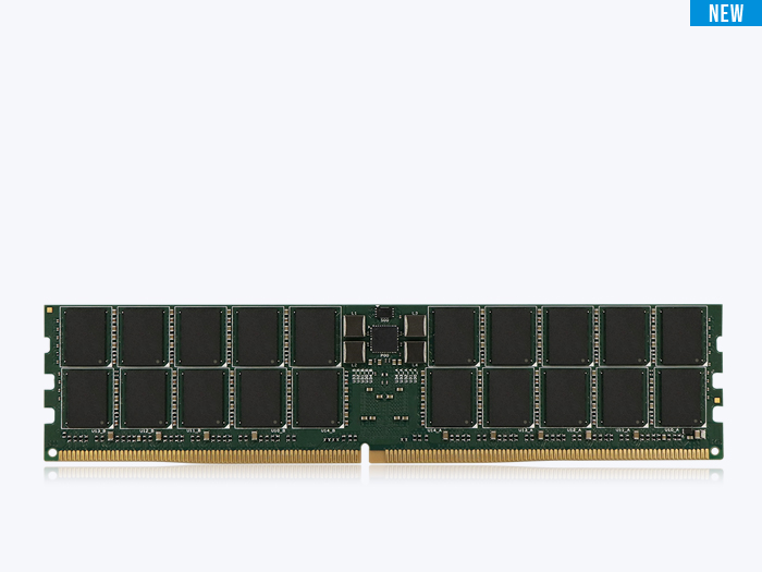
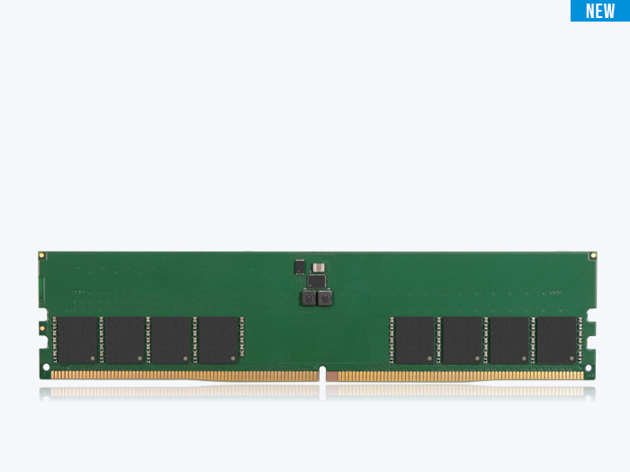
A guide to DDR5 and today’s DRAM module form factors — RDIMM, UDIMM, LRDIMM, SO-DIMM, CUDIMM, MRDIMM, CAMM2 and LPCAMM2 — what actually changed inside DDR5, and how to choose a module for an industrial or embedded design where the fastest part is seldom the right one.
Key Takeaways
- DDR5 is not simply a faster DDR4 — it is a re-architected module. JEDEC’s DDR5 standard spans 4800 to 8800 MT/s, splits each DIMM into two independent 32-bit sub-channels, moves power regulation onto the module with an on-board PMIC, and adds on-die ECC that corrects single-bit errors inside the DRAM die. On-die ECC is a chip-level reliability feature — it does not protect data on the bus, and it does not make a module an ECC module.
- At DDR5-6400 and above, the module needs its own clock. JEDEC’s CUDIMM (Clocked Unbuffered DIMM) and CSODIMM add a Client Clock Driver (CKD) that regenerates the clock signal on the module, holding signal integrity at speeds where the CPU’s memory controller alone can no longer guarantee it.
- Form factor now encodes intent, not just size. RDIMM and MRDIMM target server bandwidth and capacity; CUDIMM/CSODIMM target high-speed client systems; CAMM2 and LPCAMM2 target thin, serviceable, low-power designs — so the module type you specify says as much about the workload as the DRAM generation does.
- MRDIMM doubles per-channel bandwidth by running two ranks at once. A Gen1 MRDIMM at 8800 MT/s delivers about 70.4 GB/s per channel versus 51.2 GB/s for a DDR5-6400 RDIMM, which is why it is aimed at AI and HPC servers rather than desktops.
- The right module for an industrial design is rarely the fastest one. Wide operating temperature (−40°C to 85°C), very-low-profile height, system-level ECC, and long-term availability usually matter more than peak MT/s.
- If your platform is on DDR4 and meeting its targets, there is no engineering case for moving it to DDR5. For many embedded systems still in production, DDR4 — and older generations — remains the correct specification.
What this guide covers
If you are specifying memory for a new design — or trying to understand why a laptop now ships with a flat module bolted to the board instead of a stick in a slot — the vocabulary has moved on. DDR4 is no longer the newest generation, “DIMM” no longer means one thing, and a handful of module types that did not exist a few years ago now decide whether a system hits its target speed at all.
This guide starts with the fundamentals — what RAM is, how DRAM differs from SRAM, and how the DDR generations relate — then works up to DDR5 and the current module form factors: RDIMM, UDIMM, LRDIMM, SO-DIMM, the new clocked CUDIMM/CSODIMM, the server-focused MRDIMM, and the compression-attached CAMM2 and LPCAMM2. It closes with where high-bandwidth memory (HBM) fits, and how to choose a module for an industrial or embedded system, where the fastest part is seldom the right one.
What is RAM, and how is it different from storage?
Random-access memory (RAM) is the working memory a system uses while it is running. It holds the data and instructions the CPU is actively using, and it is fast and directly addressable — the processor can reach any location in roughly the same amount of time, which is what “random access” means.
RAM is volatile: it loses its contents when power is removed. That is the line between memory and storage. Storage — an SSD, an eMMC device, an SD card — is non-volatile and retains data without power, but it is slower and is reached in blocks rather than by direct address. A system reads a program from storage into RAM to run it, and writes results back to storage to keep them. More RAM means the CPU fetches from the slower storage device less often, so the two are sized together, not traded off against each other.
There is also read-only memory (ROM): non-volatile memory that holds the code a system needs to start before the operating system loads. Once boot is complete, active work happens in RAM.
DRAM vs. SRAM: two ways to hold a bit
The two main types of RAM are dynamic RAM (DRAM) and static RAM (SRAM), and the difference is physical.
A DRAM cell stores one bit as charge in a capacitor, controlled by a single transistor. Capacitors leak, so the charge fades within milliseconds and every cell must be refreshed — read and rewritten — continuously to retain its data. That refresh overhead is the price of DRAM’s biggest advantage: one transistor and one capacitor per bit is compact and cheap to manufacture at scale, which is why DRAM is used as main memory.
An SRAM cell holds its bit in a latch built from four to six transistors and needs no refresh as long as power is applied. That makes SRAM faster and lower-latency, but far larger and more expensive per bit. Its role is small, speed-critical memory — most visibly the CPU’s cache. In practice the two are complementary: SRAM for the caches closest to the core, DRAM for the large main-memory pool. This guide is about DRAM and the modules it is packaged on.
The DRAM generations: from SDRAM to DDR5
Modern DRAM is synchronous — its operations are tied to the system clock, so the memory controller knows exactly which clock cycle data will be ready. The first widely used form, single data rate SDRAM (SDR), transferred one word of data per clock cycle.
Double Data Rate (DDR) SDRAM roughly doubled bandwidth at the same clock frequency by transferring data on both the rising and falling edges of the clock — a technique called double pumping. Each DDR generation has extended that idea with higher signaling rates, wider internal parallelism, and lower operating voltage. The generations are not backward-compatible: the connector keying and pinout change so a module cannot be seated in a socket of a different generation.
- DDR1 through DDR3 stepped transfer rates up while dropping voltage from 2.5V toward 1.35–1.5V.
- DDR4 became the mainstream standard for roughly a decade, running at 1.2V with common data rates from 2133 up to 3200 MT/s, and moved DIMMs to a 288-pin connector.
- DDR5 is the current generation. It starts at 4800 MT/s and the JEDEC standard scales to 8800 MT/s, at a lower 1.1V core voltage — and, as the next section explains, it changes far more than the speed.
Data rate here is quoted in MT/s (mega-transfers per second), not MHz. Because DDR moves data twice per clock cycle, a module on a 3200 MHz clock performs 6400 MT/s of transfers — the MT/s figure is the one that maps to bandwidth.
What actually changed in DDR5
DDR5 is best understood as a redesign of the memory module, not just a higher clock. Four changes matter most.
- Two independent sub-channels per module. A DDR4 DIMM presents one 72-bit channel (64 data bits plus 8 for ECC). A DDR5 DIMM splits that into two independent 32-bit sub-channels (40 bits with ECC). Each has its own command/address bus, so the memory controller manages two narrower conversations instead of one wide one — which, combined with a longer burst length, improves efficiency for the smaller, more concurrent accesses that modern multi-core and accelerator workloads generate.
- On-die ECC. DDR5 adds error correction inside the DRAM die itself, correcting single-bit errors before data leaves the chip. This is a manufacturing-reliability feature — it lets DRAM makers ship denser dies on advanced process nodes by cleaning up the bit errors those nodes produce. It is distinct from system-level ECC, which protects data across the bus between module and controller and reports correctable errors to the host. A module can have on-die ECC without being a system-ECC module, and every DDR5 module has on-die ECC, so its presence tells you nothing about whether a module is an ECC part.
- Power management moved onto the module. DDR5 relocates voltage regulation from the motherboard to a Power Management IC (PMIC) on the module itself, regulating from a 12V (server-class) or 5V (client-class) input to the voltages the DRAM needs. Putting regulation next to the load tightens voltage tolerance across the module — which matters more as signaling rates climb and noise margins shrink. It also concentrates more of a module’s reliability in parts carried on the module itself, which is why validating a DDR5 module as a finished, thermally cycled unit — not just trusting the individual components — carries more weight than it did for DDR4.
- The clock problem at high speed. As DDR5 pushes past 6400 MT/s, the clock signal degrades over the module traces faster than the CPU’s integrated memory controller can reliably compensate for. That is the problem the new clocked module types were created to solve.
DDR4 vs. DDR5 at a glance
| Dimension | DDR4 | DDR5 |
|---|---|---|
| JEDEC data rates | 1600–3200 MT/s | 4800–8800 MT/s |
| Core voltage | 1.2V | 1.1V |
| Channel structure per DIMM | One 72-bit channel (64 data + 8 ECC) | Two independent 32-bit sub-channels (40 bits each with ECC) |
| On-die ECC | No | Yes, on every module |
| Power regulation | On the motherboard | PMIC on the module |
| DIMM connector | 288-pin | 288-pin, different keying and pinout — not interchangeable |
| Clock driver on module | No | Required on CUDIMM/CSODIMM at 6400 MT/s and above |
| Module types in current use | RDIMM, UDIMM, LRDIMM, SO-DIMM, Mini-DIMM | RDIMM, UDIMM, LRDIMM, SO-DIMM, CUDIMM, CSODIMM, MRDIMM, CAMM2 |
| ATP industrial range | Up to 3200 MT/s; RDIMM 4 GB–128 GB; 0°C to 85°C or −40°C to 85°C |
Up to 7200 MT/s, with 6400 and 7200 MT/s now shipping; RDIMM 16 GB–256 GB; 0°C to 85°C or −40°C to 85°C |
RAM module form factors, and how to read them
A DRAM module (“stick”) is one or more DRAM chips on a small PCB with a standard edge connector. The dominant package is the DIMM (Dual In-line Memory Module) — “dual in-line” because it has independent contacts on both faces of the connector. The obsolete SIMM it replaced had a narrower bus and contacts that were electrically common across both faces. DDR4 and DDR5 DIMMs both use a 288-pin connector, but the pin assignment and the keying notch differ between the two generations, which is why a DDR5 module will not seat in a DDR4 board.
Within the DIMM family, the differences come down to how — and whether — the module buffers the signals between the DRAM chips and the memory controller. That buffering choice is what each acronym encodes.
| Module type | What it does | Typical use |
|---|---|---|
| UDIMM (Unbuffered DIMM) | Commands pass directly from the controller to the DRAM. Lowest latency and cost; less electrical stability at high capacity. | Desktops, workstations, embedded systems |
| RDIMM (Registered DIMM) | A register buffers command, address, and clock signals, reducing electrical load on the controller for greater stability and capacity. Adds about one clock cycle of latency. | Servers, high-reliability systems |
| LRDIMM (Load-Reduced DIMM) | A registering clock driver buffers command, address, and clock, and data buffers re-drive the data lines, so the controller sees only the buffers rather than the DRAM chips. Pushes capacity higher than RDIMM at heavy memory loading. | Maximum-capacity servers |
| CUDIMM (Clocked Unbuffered DIMM) | A UDIMM with an added Client Clock Driver (CKD) that regenerates the clock on the module. | High-speed client systems, DDR5-6400 and up |
| CSODIMM (Clocked SO-DIMM) | The CUDIMM design in the smaller SO-DIMM footprint. | Laptops, mini-PCs, compact embedded systems |
| MRDIMM (Multiplexed Rank DIMM) | Runs two ranks simultaneously through a multiplexing buffer, doubling data per channel beyond standard DDR5 rates. | AI/HPC servers |
What is a CUDIMM, and when does a system need one?
A CUDIMM is a Clocked Unbuffered DIMM: a standard unbuffered DDR5 module with one added component, the Client Clock Driver (CKD), which receives the clock from the memory controller and regenerates a clean copy on the module.
Regenerating the clock reduces jitter and holds signal integrity at elevated data rates. JEDEC set DDR5-6400 as the point where a redriven clock becomes necessary — above it, an unbuffered module loses stability. The controller must still support the target data rate, since data and command lines remain unbuffered; what the CKD changes is that the clock no longer degrades across the module, so the module is not held back by the quality of the controller’s clock output. The CSO-DIMM (Clocked Small Outline DIMM) is the same idea in the smaller SO-DIMM footprint, for laptops, mini-PCs, and compact embedded systems.
Because only the clock is buffered, a CUDIMM keeps the low latency of a UDIMM while gaining high-speed stability that used to require registered memory. For a system running at 5600 MT/s or below in a room-temperature enclosure, a standard UDIMM is sufficient and costs less.
The industrial case adds a second reason beyond raw speed. A module that has to hold its rated speed at −40°C and again at 85°C spends timing margin on temperature that a desktop module never has to, and a regenerated clock is margin the design does not have to find elsewhere. ATP’s CUDIMM and CSO-DIMM run at 6400 and 7200 MT/s — at and above the threshold where JEDEC requires a clocked module — in both commercial (0°C to 85°C) and wide-temperature (−40°C to 85°C) grades, which puts high-speed DDR5 within reach of embedded designs that standard client modules are not built for.
The bandwidth module: MRDIMM
MRDIMM (Multiplexed Rank DIMM) is a server-class module built for one goal: bandwidth. It uses a multiplexing buffer to run two ranks of DRAM simultaneously and interleave their output, so the module transfers roughly twice the data per channel of a conventional DIMM built from the same DRAM. JEDEC’s first-generation MRDIMM runs at 8800 MT/s — about 70.4 GB/s per channel, against 51.2 GB/s for a DDR5-6400 RDIMM — and JEDEC’s Gen2 roadmap targets 12800 MT/s, with the supporting buffer standards already published. This is memory for feeding large datasets to CPUs and accelerators in AI and HPC servers; it is not a desktop part, and it depends on platform support in the CPU and firmware.
The small and space-constrained modules
Not every system has room for a full-height DIMM, and several form factors exist for tighter designs:
- SO-DIMM (Small Outline DIMM) is the long-standing compact module, at 69.6 mm long against a standard DIMM’s 133.35 mm — roughly half the length — and is used in laptops, mini-PCs, and a large share of embedded and industrial systems.
- VLP (Very Low Profile) and ULP (Ultra-Low Profile) are reduced-height standard-length modules for chassis where vertical clearance is limited, such as blade servers and rack-dense or fanless embedded enclosures. A standard DDR4 DIMM stands 31.25 mm tall; a VLP version cuts that to 18.75 mm.
- Mini-DIMM is a shortened module — about 80 mm long, against a standard DIMM’s 133.35 mm — for space-constrained systems, available in both registered (Mini-RDIMM) and unbuffered (Mini-UDIMM) forms.
ATP module form factors
These are the DDR4 module outlines ATP builds to. The module lengths are set by the JEDEC form factor rather than the DRAM generation, so a DDR5 DIMM and SO-DIMM share the same 133.35 mm and 69.6 mm outlines — what changes between generations is the keying and pinout, not the footprint.
| Module | Size (L × H, mm) | Image |
|---|---|---|
| DDR4 RDIMM ECC — standard | 133.35 × 31.25 | 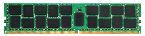 |
| DDR4 RDIMM ECC — Very Low Profile (VLP) | 133.35 × 18.75 |  |
| DDR4 UDIMM ECC | 133.35 × 31.25 | 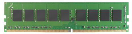 |
| DDR4 SO-DIMM ECC | 69.6 × 30 | 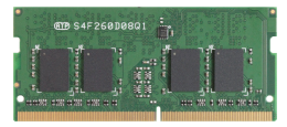 |
| DDR4 Mini-DIMM, unbuffered ECC — VLP | 80 × 18.75 | 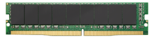 |
Non-ECC versions are also available. For current densities, speeds, and operating temperature options, see the ATP DDR4 and ATP DDR5 product pages.
CAMM2 and LPCAMM2: the compression-attached modules
The newest form factor is a departure from the edge-connector DIMM entirely. CAMM2 (Compression Attached Memory Module, version 2) — standardized by JEDEC as JESD318 — replaces the row of edge contacts with a grid of contacts, similar to a CPU land grid, that the module is compressed onto so it lies flat and parallel to the board rather than standing perpendicular in a slot.
That geometry buys three things: a thinner overall profile, more clearance around the socket, and a shorter, more uniform electrical path that helps at high signaling rates. The standard defines two variants. DDR5 CAMM2 targets performance notebooks and mainstream desktops. The LPDDR5/5X variant — commonly called LPCAMM2 — brings low-power DRAM into a serviceable module: it delivers the efficiency of soldered-down LPDDR while remaining replaceable and upgradeable, which soldered memory is not. LPCAMM2 targets thin-and-light notebooks and is also being adopted in parts of the low-power server segment.
Low-power DRAM: LPDDR5X
LPDDR5X is the mobile and edge branch of the DRAM family — a low-power variant optimized for battery-constrained and thermally constrained systems. JESD209-5C defines LPDDR5X up to 8533 MT/s, with shipping parts and LPCAMM2 implementations reaching higher, and it delivers meaningfully better energy efficiency than standard DDR — mainly through lower I/O voltage and architectural power-saving features rather than a lower core voltage. It is traditionally soldered directly to the board, which is why LPCAMM2 — a serviceable module built from LPDDR5X — is a notable change. For edge AI inference, handheld, and always-on designs where power budget and board area dominate, LPDDR5X is often the right memory even though it gives up the capacity ceiling and serviceability of a DIMM.
Where HBM fits
High Bandwidth Memory (HBM) sits outside the module conversation entirely, and it makes a useful contrast. Instead of chips on a stick in a socket, HBM stacks DRAM dies vertically and connects them through an extremely wide interface — 1024 bits per stack in HBM3E, 2048 bits in HBM4 — mounted on a silicon interposer right beside the processor or accelerator. HBM3E reaches over 1.2 TB/s of bandwidth per stack; the HBM4 standard (JESD270-4, published in 2025) pushes past 2 TB/s.
The trade-off is the mirror image of a DDR5 module. DDR5 gets its bandwidth from high speed over a relatively narrow interface, on a replaceable module you can add capacity to. HBM gets far higher bandwidth from an enormous interface at more modest per-pin speeds, but it is fabricated into the package, cannot be replaced or expanded, and is expensive. That is why HBM appears on GPUs and AI accelerators where bandwidth is the binding constraint, while DDR5 remains the main memory for CPUs and the vast majority of systems.
Choosing a module for an industrial or embedded design
For a design that will be built, validated, and deployed for years, the selection criteria are different from a performance desktop, and the fastest module is rarely the right answer.
Start with the environment. Standard modules are typically rated for 0°C to 85°C, which is fine for a climate-controlled cabinet but not for an outdoor enclosure, a vehicle, or an unconditioned industrial floor. A wide-temperature module is one built with ICs screened and tested to operate across −40°C to 85°C — ATP’s industrial DDR5 and DDR4 lines are offered in both ranges. Specifying wide-temp when the deployment does not need it is wasted cost, just as specifying commercial-temp for an outdoor system is a field-failure risk.
Then the mechanical envelope. Height often decides the form factor before performance does: a fanless or rack-dense enclosure may require VLP height or an SO-DIMM regardless of the bandwidth on offer.
ATP’s DDR5 modules span RDIMM (16 GB to 256 GB) plus CUDIMM, CSO-DIMM, UDIMM, and SO-DIMM in ECC and non-ECC versions (8 GB to 64 GB), reaching 7,200 MT/s, with VLP options on RDIMM, CUDIMM, and UDIMM and an integrated CKD on the clocked types. Reliability options that matter in the field — anti-sulfur protection for corrosive environments, thicker gold-plated contacts, PCB chamfer, SPD write protection — are available on request rather than assumed.
Reliability and error handling come next. On-die ECC is present across DDR5, but system-level ECC — the kind that protects data across the bus and reports correctable errors to the host — requires an ECC module and platform support. For medical, defense, transportation, and other systems where a silent bit error is unacceptable, that is a specification requirement, not an upgrade.
Availability is the criterion consumer guides omit. A module specified into a certified system may need to be sourced, unchanged, for five to ten years or longer, so long-term supply and revision control can outweigh peak speed.
This is also why DDR4 — and older generations still — remains the correct specification for many systems in production today; ATP continues to offer legacy DRAM in DDR4, DDR3, DDR2, DDR1, and legacy SDRAM form factors for that reason. If your platform is on DDR4 and meeting its targets, there is no engineering case for moving it to DDR5.
To hold quality across those long lifecycles, ATP validates from IC level up through module and finished product using automated test equipment for marginal voltage, signal frequency, clock, and command/data timing under continuous thermal cycling, and screens early-life failures with Test During Burn-In (TDBI) in a thermal chamber. For a component that has to survive years of unattended operation, that screening is the difference between a rated spec and a spec that holds in the field.
Conclusion
DDR5 changed more than the number on the module label. Two sub-channels, on-die ECC, an on-board PMIC, and a clock driver above 6400 MT/s mean the form factor you specify now carries as much design intent as the DRAM generation does — and it also means more of a module’s reliability is carried on the module itself. For an industrial or embedded design, that shifts the selection order: operating temperature range, height limit, system-level ECC, and long-term availability decide the part before peak MT/s does, and for many systems already in production DDR4 or an earlier generation remains the correct specification.
ATP builds industrial DRAM across that whole range — DDR5 RDIMM, CUDIMM, CSO-DIMM, UDIMM and SO-DIMM in commercial and wide-temperature grades, alongside DDR4 and legacy generations for long-lifecycle platforms. Engage ATP early in the design phase so the module can be matched to your actual temperature range, mechanical envelope, ECC requirement, and sourcing window rather than retrofitted to them. Contact ATP or reach out to a distributor or representative in your area to review your requirements.
Frequently Asked Questions (FAQ)
Q1: What is the difference between DDR4 and DDR5?
A: DDR5 is the newer DRAM generation: it starts at 4800 MT/s and scales to 8800 MT/s versus DDR4’s typical 2133–3200 MT/s, runs at 1.1V instead of 1.2V, splits each module into two independent 32-bit sub-channels, adds on-die ECC, and moves power regulation onto the module with a PMIC. The two are not interchangeable — DDR5 modules use different keying and will not fit a DDR4 socket, even though both use a 288-pin connector.
Q2: Is DDR4 still worth using in 2026?
A: Yes, for many systems. If a platform is built on DDR4 and meeting its performance targets, there is no engineering case for moving it to DDR5 — the migration means a new memory controller, new validation, and a new bill of materials for a benefit the workload may not use. DDR4 also has the deeper advantage for long-lifecycle designs: a mature, well-characterized ecosystem and long-term supply, which matter more than peak MT/s when a certified system has to be sourced unchanged for a decade. DDR5 is the right answer for a new platform being designed now; it is not automatically the right answer for an existing one.
Q3: What is a CUDIMM, and do I need one?
A: A CUDIMM (Clocked Unbuffered DIMM) is a DDR5 module with an added Client Clock Driver (CKD) that regenerates the clock signal on the module to keep it stable at high speed. JEDEC set DDR5-6400 as the point where a clocked module becomes necessary, so at 6400 MT/s and above the CKD is what maintains signal integrity — ATP’s CUDIMM and CSO-DIMM run at 6400 and 7200 MT/s for that reason. At 5600 MT/s and below, a standard UDIMM is sufficient for a room-temperature system and costs less.
Q4: Can I use a CUDIMM in a normal DDR5 UDIMM slot?
A: Physically yes — a CUDIMM uses the same 288-pin DDR5 UDIMM connector and keying — but the platform decides whether it runs in clocked mode. Boards and BIOS that support CUDIMM operation drive the module through its CKD; those that do not may run the module in bypass mode at a standard UDIMM data rate, or may not support it at all. Check the motherboard or platform documentation for CUDIMM support before specifying one, and note that the memory controller must still support the target data rate, since the CKD buffers only the clock, not the data and command lines.
Q5: What is the difference between MRDIMM and RDIMM?
A: An RDIMM buffers command, address, and clock signals to improve stability and capacity, and runs at standard DDR5 data rates. An MRDIMM adds a multiplexing buffer that runs two ranks at once, roughly doubling bandwidth per channel — a Gen1 MRDIMM delivers about 70.4 GB/s per channel at 8800 MT/s versus 51.2 GB/s for a DDR5-6400 RDIMM. MRDIMM is a server and AI part that requires platform support; RDIMM is the broader-compatibility server standard.
Q6: What are CAMM2 and LPCAMM2?
A: CAMM2 (Compression Attached Memory Module, version 2) is a JEDEC form factor, standardized as JESD318, that replaces the DIMM’s edge connector with a flat grid of contacts, so the module lies parallel to the board — thinner, with better clearance and shorter signal paths. LPCAMM2 is the LPDDR5X version: it delivers low-power memory efficiency in a serviceable, replaceable module, which soldered-down LPDDR cannot offer.
Q7: Does DDR5 still need ECC memory if it already has on-die ECC?
A: Yes, if the system needs to detect and report memory errors. On-die ECC is present on every DDR5 module and corrects single-bit errors inside the DRAM die, but it is a manufacturing-reliability feature: it works silently, and its protection ends at the chip boundary. System-level ECC is what protects data across the bus between module and controller and reports correctable errors to the host, and it requires both an ECC module and platform support. For medical, defense, transportation, and other systems where a silent bit error is unacceptable, on-die ECC alone does not satisfy the requirement. For a kiosk or signage player in a controlled environment, non-ECC DDR5 is adequate and costs less.
Q8: Why does DDR5 have a PMIC on the module?
A: DDR5 moves voltage regulation from the motherboard onto the module so that regulation sits next to the load it serves, which tightens voltage tolerance across the module as signaling rates climb and noise margins shrink. The PMIC regulates from a 12V input on server-class modules or 5V on client-class modules down to the voltages the DRAM needs. One practical consequence for specifiers: more of a module’s reliability now depends on components carried on the module itself, so validating the finished, thermally cycled module matters more than it did with DDR4.
Q9: What is a wide-temperature DRAM module?
A: A wide-temperature DRAM module is a memory module built with ICs screened and tested to operate reliably from −40°C to 85°C, compared with the 0°C to 85°C rating of standard commercial modules. The wide range covers both extremes an industrial system meets in the field: sustained heat inside a sealed, fanless enclosure, and sub-zero cold starts in outdoor, roadside, or vehicle-mounted installations. If the enclosure is climate-controlled and easy to service, a standard 0°C to 85°C module is adequate and costs less.
Q10: What is the difference between HBM and DDR5?
A: HBM gets its bandwidth from an extremely wide interface — 1024 bits per stack in HBM3E, 2048 bits in HBM4 — with the DRAM stacked vertically and mounted on a silicon interposer next to the processor, reaching over 1.2 TB/s and past 2 TB/s per stack respectively. DDR5 gets its bandwidth from high speed over a narrower interface on a replaceable module. The trade-off is serviceability and cost: HBM is fabricated into the package and cannot be replaced or expanded, which is why it appears on GPUs and AI accelerators where bandwidth is the binding constraint, while DDR5 remains main memory for CPUs and most systems.
Q11: Which DRAM configuration is best for embedded edge computing systems?
A: For most embedded edge computing systems, the best configuration is a wide-temperature (−40°C to 85°C) ECC module in a compact form factor — a CSO-DIMM or SO-DIMM where space is tight, an ECC UDIMM or CUDIMM where a standard slot is available. Those three attributes answer the constraints that define edge deployments: the systems run unattended, so ECC catches errors before they become site visits; the enclosures are compact, so a SO-DIMM at 69.6 mm or a VLP module at 18.75 mm height often decides the choice before speed does; and the environment is rarely climate-controlled. Edge servers needing capacity beyond a single-module limit move to RDIMMs, which reach 256 GB per module in ATP’s DDR5 line.
Q12: Which DRAM module should I choose for an industrial system?
A: Start with the operating environment and mechanical envelope, not the speed. Confirm the temperature range you need (0°C to 85°C for controlled cabinets, −40°C to 85°C for outdoor, vehicle, or unconditioned deployments), the height limit (VLP or SO-DIMM for tight enclosures), and whether the application requires system-level ECC. Then weigh long-term availability, since a module in a certified system may need to be sourced unchanged for a decade — which is also why DDR4 remains the right choice for many systems still in production.