Introduced 10 years ago, the NVMe specifications took NAND flash storage to unprecedented levels of speed and performance, with 6X the throughput and 7X lower latency than Serial ATA 6 Gbps (also commonly known as SATA III). Storage devices supporting the NVMe protocol connect to the host system using the PCI Express (PCIe) bus, leveraging its excellent features for scalability, low latency and fast performance. [For a more detailed comparison on NVMe vs. SATA, please refer to a previous blog article here.]
NAND flash storage supporting the NVMe protocol comes in several form factors using different interfaces, which we will discuss in this article.
M.2 Cards/Modules
M.2 (pronounced M-dot-two) is a specification for internal expansion cards. It was formerly known as the Next Generation Form Factor (NGFF) and was created as a successor of the mSATA standard.
This specification allows flexible physical forms. Modules can come in different widths and lengths, with connectors supporting both legacy SATA interface (via AHCI) and PCIe interface (via NVMe). To ensure compatibility with the host system, M.2 card connectors are uniquely keyed depending on the card’s purposes or capabilities.
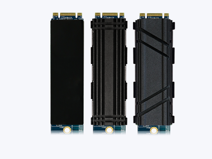
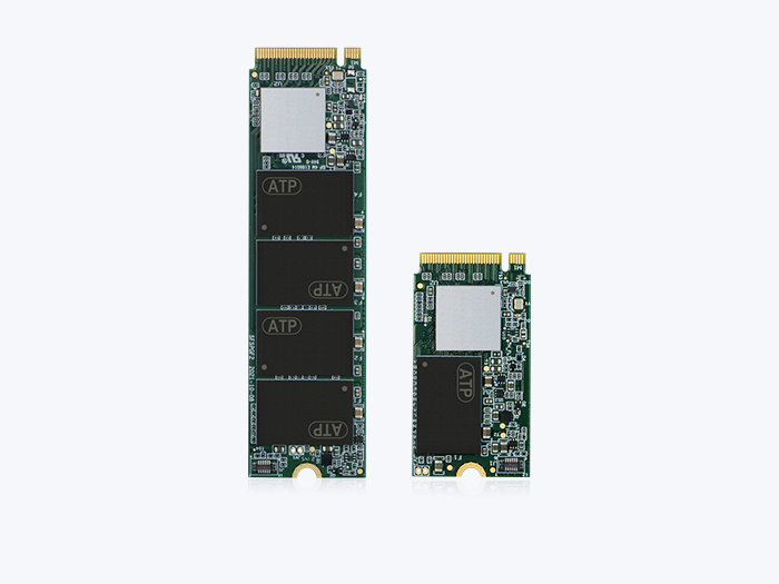
ATP’s NVMe-based M.2 solid state drives come in three forms:
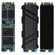
- M.2 2280. Each module measures 22 mm wide and 80 mm long, and comes in double-sided configuration, which means that components are installed on both top and bottom sides of the module.
The following table compares the physical appearance and key specifications of ATP’s NVMe-based M.2 2280 SSDs.
*Case Temperature, the composite temperature as indicated by SMART temperature attributes.
Table 1. ATP M.2 2280 NVMe SSD Specifications
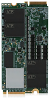
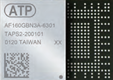
- M.2 Type 1620 HSBGA. Heatsink ball grid array (HSBGA) SSDs are ATP’s tiniest flash storage solutions supporting the NVMe protocol. As soldered-down solutions, they are secure in place even during constant vibrations and rigorous operations. The HSBGA measures 16 (L) x 20 (W) x 1.6 (H) mm) and use high-speed PCIe 3.0 interface x4 lanes and NVMe protocol to deliver up to 32 Gb/s bandwidth at 8 Gb/s per lane.
*Case Temperature, the composite temperature as indicated by SMART temperature attributes.
Table 2. ATP NVMe M.2 HSBGA SSD Specifications
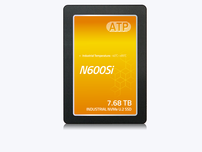
2.5” U.2
SSDs with the U.2 (pronounced U-dot-two) connector support the PCIe interface via the NVMe protocol. Formerly known as SFF-8639, U.2 uses a total of four PCIe lanes for a maximum theoretical bandwidth of up to 32 Gbps. ATP’s NVMe U.2 SSDs are similarly sized as 2.5” SATA SSDs. They are designed with aluminum housing for better heat dissipation.
The following figure compares the physical appearance of the 2.5” with U.2 SSDs and shows the U.2 connector.
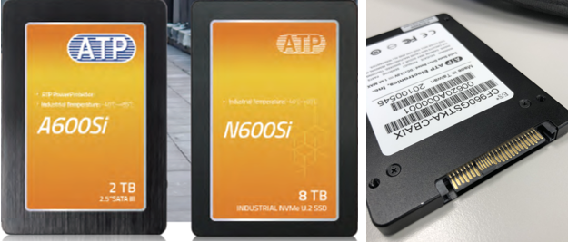
Figure 1. From left: 2.5” SATA SSD, U.2 SSD and U.2 connector
Table 3. ATP NVMe U.2 SSD Specifications
EDSFF
The Enterprise and Datacenter SSD Form Factor (EDSFF) family of specifications was developed by a group of 15 companies to meet the increasing data generation and consumption requirements of data center storage. EDSFF SSDs come in different form factors but share the same NVMe protocol, PCIe interface, edge connector, and pinout and functions.
EDSFF form factors are listed below. Each form factor has different variants. For more information, please visit the SNIA website.
- E1.L (EDSFF 1U Long). It was inspired by Intel’s “ruler” form factor, which offered capacities that were unavailable from other SSD configurations. It is designed for high-capacity and dense storage use cases. As its name implies, E.1L was “developed to maximize capacity per drive and per rack unit in a 1U server or storage array.”
- E1.S (EDSFF 1U Short). The E1.2 is more like the M.2 and U.2 – small and compact, just a bit longer to accommodate more flash memory. It is also hot-pluggable, unlike the M.2.
- EDSFF E3.L and E.3S. These form factors are optimized for 2U servers and are similar to 2.5” SSDs. The E3 connector can support up to x16 PCIe lanes, while most SSDs today support up to x4 lanes.
Conclusion
The NVMe protocol has enabled NAND flash storage devices to break the barriers of SATA. As the world continues to generate more data, ATP takes advantage of technological advances to make sure that your data is stored safely, accessed speedily, and transformed into actionable insight when needed.
As a true manufacturer, we can customize hardware, firmware and software to provide the most suitable solutions for your memory and storage needs. For more information on ATP’s extensive range of products and services, please visit https://www.atpinc.com/ or contact an ATP Representative in your area.