e.MMC (Embedded MultiMediaCard) integrates NAND flash, a controller, and the MMC interface in one soldered BGA package — managed NAND at the component level. This primer explains what e.MMC is, how it manages its own flash, how it differs from an SSD, and when an embedded system should choose e.MMC instead of an industrial SSD.
Key Takeaways — e.MMC or an Industrial SSD for Your Embedded System?
Use e.MMC when an embedded system needs soldered-down storage for boot, application code, and local data up to 256 GB in a space- or vibration-constrained design; move to an industrial SSD when capacity, sustained throughput, or field serviceability outgrow a single BGA package.
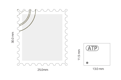
- e.MMC (Embedded MultiMediaCard) integrates NAND flash, a flash controller, and the MMC interface in one 153-ball FBGA with an 11.5 × 13 mm footprint, reflow-soldered to the board — wear leveling, bad block management, and error correction run inside the package, and there is no connector to work loose under vibration.
- An SSD manages its NAND too: it pairs raw NAND chips with a discrete controller on the drive’s circuit board. The e.MMC-versus-SSD choice is about integration level, interface ceiling, and capacity — not about which device is “managed.”
- The interface sets the ceiling. e.MMC 5.1’s HS400 mode tops out at 400 MB/s of bus bandwidth, and ATP’s current industrial e.MMC line spans 10 GB to 256 GB in 3D TLC and pSLC-mode configurations. SATA SSDs reach 550 MB/s and PCIe NVMe SSDs go well beyond, with capacities to match.
- Temperature rarely decides between them: ATP’s industrial e.MMC and industrial SSDs share the −40°C to 85°C operating rating. Board space, capacity, throughput, and the service model are the constraints that actually separate the two.
- Not every embedded design needs the industrial grade. ATP’s commercial e.MMC (−25°C to 85°C) covers climate-controlled, low-duty systems at lower cost — while workloads that sustain heavy writes or need more than 256 GB are industrial SSD territory from the start.
What Is e.MMC?
Embedded MultiMediaCard, or e.MMC, is an advanced managed NAND flash storage solution soldered directly to the motherboard. It integrates the following components in the same IC package:
- MMC interface
- NAND flash memory
- NAND flash controller
Typical SSDs are built from “raw” NAND flash chips managed by a discrete controller on the drive’s circuit board. e.MMC takes the same functional blocks and integrates them in a single IC package — it is “managed” NAND at the component level, so flash management travels with the part itself.
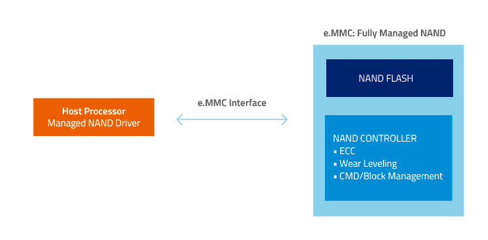
The integrated package design offers the following benefits:
- Internal NAND management frees the host from having to perform low-level flash background operations such as wear leveling, bad block management, error correction and other functions.
- Simplified qualification process reduces time-to-market.
- High throughput support for large data transfers delivers the performance required by data-intensive applications.
- Low power consumption suits battery- and thermally-constrained systems.
- Simplified memory interface design allows e.MMC to be extremely compact and provides support for future flash storage devices. The small footprint fits space-constrained boards; its soldered BGA construction withstands shock and vibration in automotive and industrial environments.
Usage
Today, e.MMC’s main home is embedded systems: industrial automation, automotive applications such as infotainment, aerospace/avionics, Internet of Things (IoT) devices, and other designs that need compact, soldered-down storage. Its small footprint and simple integration first made it a mainstay of mobile devices such as smartphones, tablets and laptops — the same properties that now make it a preferred choice for space-constrained embedded designs.
Latest Standard
JEDEC published e.MMC 5.1 (JESD84-B51) in February 2015; the standard has since been revised as JESD84-B51A (January 2019) and, most recently, JESD84-B51B (September 2025). The table below compares the features introduced across recent e.MMC versions.
| Features | Version / Year | ||
|---|---|---|---|
| 4.51 (2012) | 5.0 (2013) | 5.1 (2015) | |
| Max. Bus Speed Mode | HS200 | HS400 | |
| Max. Data Transfer | 200 MB/s | 400 MB/s | |
| Max. Clock Frequency | 200 MHz SDR | 200 MHz DDR | |
| Command Queuing | — | ✓ | |
| Cache Barrier | — | ✓ | |
| Enhanced Data Strobe | — | ✓ | |
| Cache Flushing Report | — | ✓ | |
| Secure Write Protection | — | ✓ | |
| Data Strobe | — | ✓ | |
| Data Bus Width* | 4/8 bits | 8 bits | |
| Production State Awareness | — | ✓ | |
| Field Firmware Update | — | ✓ | |
| Device Health Report | — | ✓ | |
Table 1. Specifications comparison of different e.MMC versions. *Versions 4.51/5.0/5.1 support all data bus widths (1/4/8 bits) when providing backward compatibility for lower speeds such as those of legacy MMC cards, high-speed SDR and high-speed DDR.
Version Change Highlights
| v4.51 to v5.0 | v5.0 to v5.1 |
|---|---|
| HS400 mode raised the maximum interface data transfer rate from 200 MB/s to 400 MB/s. | Command Queuing and Cache Barrier added to enhance random read/write performance. |
| Production State Awareness (PSA) introduced to secure pre-load data during the e.MMC/PCB soldering process. | Cache Flushing Report added to ensure the data integrity on cache blocks. |
| Field Firmware Update (FFU) introduced to allow features enhancement in the field by updating the e.MMC firmware that is fixed on a PCB. | Enhanced Strobe in HS400 Mode added to facilitate faster synchronization between the host and the e.MMC device. |
| Device Health Report introduced to monitor the health condition of an e.MMC. | Secure Write Protection added to ensure that only trusted entities can protect or unprotect the e.MMC device. |
How Fast Is e.MMC 5.1?
According to the JESD84-B51 standard, e.MMC v5.1 supports the following bus speed modes and clock frequencies.
| Mode Name | Data Rate | I/O Voltage (volts) | Bus Width (bits) | Frequency (MHz) | Max. Data Transfer (MB/s, implies x8 bus width) |
|---|---|---|---|---|---|
| HS400 | Dual | 1.8/1.2 V | 8 | 0–200 MHz | 400 MB/s |
| HS200 | Single | 1.8/1.2 V | 4, 8 | 0–200 MHz | 200 MB/s |
| High-Speed DDR | Dual | 3/1.8/1.2 V | 4, 8 | 0–52 MHz | 104 MB/s |
| High-Speed SDR | Single | 3/1.8/1.2 V | 1, 4, 8 | 0–52 MHz | 52 MB/s |
| Backward Compatibility with Legacy MMC card | Single | 3/1.8/1.2 V | 1, 4, 8 | 0–26 MHz | 26 MB/s |
Table 2. e.MMC 5.1 bus speed modes and clock frequencies.
How Is e.MMC Different from an SSD, Memory Card, or UFS?
How is e.MMC different from other NAND flash storage products such as solid state drives (SSD), memory cards and universal flash storage (UFS)? Although storage products all use NAND flash memory chips, they are different in many ways aside from their physical appearance. Information on this table is based on ATP product specifications.
| Feature | e.MMC | Memory Cards | UFS** | SSD |
|---|---|---|---|---|
| Protocol | MMC | SD | SCSI | AHCI (SATA); NVMe |
| Interface | HS400 | UHS-I/UHS-II* | Serial Interface | SATA; PCIe |
| Form Factor(s) | 153-pin FBGA embedded (0.55 mm pitch) | SD/microSD | Card (removable); BGA (embedded) | 2.5″ drives; M.2; eSATA; SlimSATA; mSATA; eUSB |
| NAND Flash Type | Managed | Managed | Managed | Raw NAND, managed by a discrete drive-level controller |
| Data Transfer Speed (Max.) | 400 MB/s | UHS-I: 104 MB/s UHS-II: 312 MB/s UHS-III: 624 MB/s |
2-lane gear 2: 5.8 Gb/s 2-lane gear 3: 11.6 Gb/s |
SATA: 550 MB/s PCIe: 32 Gb/s (Gen3, x4 lane) |
| Dimensions L × W × H (mm) | 11.5 × 13 × 1.3 | SD: 32 × 24 × 2.1 microSD: 15 × 11 × 1.0 |
11.5 × 13 × 1.0 | 2.5″: 100.0 × 69.9 × 9.2 M.2 2242: 42 × 22 × 3.5 M.2 2260: 60 × 22 × 3.5 M.2 2280: 80 × 22 × 3.5 SlimSATA: 54 × 39 × 4 mSATA: 50.8 × 29.85 × 3.4 eUSB: 36.9 × 26.6 × 9.5 |
Table 3. Key differences of e.MMC from other NAND flash storage products. *Ultra High Speed bus interface. **UFS availability TBA.
When Should Embedded Systems Use e.MMC Instead of an Industrial SSD?
Use e.MMC when the storage job is boot code, the operating system, application binaries, and local data at capacities up to 256 GB, in a design where board space is tight, vibration is constant, or the power budget is small; choose an industrial SSD when the system needs more capacity, more sustained throughput, or storage that a technician can replace without reworking the board. Table 3 above shows the specification gap between the two — the decision itself comes down to four questions about your system: how much board area is available, whether the unit vibrates in service, how much data must move and how fast, and who will service the device after deployment.
e.MMC answers the first two questions on architecture alone. The entire storage subsystem — NAND flash, controller, and MMC interface — occupies a single 153-ball FBGA with an 11.5 × 13 mm footprint, reflow-soldered to the board, so there is no connector to fret or work loose and no drive bay to design around. Because the controller sits inside the package, wear leveling, bad block management, and error correction happen internally (Figure 1), and the host integrates one set of BGA pads instead of a storage subsystem. ATP’s industrial e.MMC carries this architecture across −40°C to 85°C, with 3D TLC configurations from 32 GB to 256 GB for capacity and pSLC-mode configurations from 10 GB to 80 GB where write endurance matters more; the smaller-footprint e.MMC line extends the same approach to boards where even the standard package is generous.
The interface draws the boundary on the other two questions. HS400 gives e.MMC 400 MB/s of bus bandwidth — ATP’s parts are rated up to 310 MB/s sequential read and 240 MB/s sequential write, measured in ATP’s proprietary test environment without file system overhead — which comfortably covers booting, application loading, configuration, and logging, but not sustained high-bitrate recording or large AI datasets. By this article’s own comparison, a SATA SSD reaches 550 MB/s and PCIe NVMe goes further still, at drive-level capacities e.MMC does not reach. Between the two sits ATP’s PCIe NVMe M.2 1620 HSBGA SSD, which keeps the soldered, vibration-resistant BGA architecture while moving to the NVMe interface. And where the maintenance plan calls for storage that field staff swap on schedule, a socketed M.2 industrial SSD or a removable industrial memory card is the more honest fit than any soldered device. Both paths hold the same temperature line — −40°C to 85°C is available on ATP e.MMC and industrial SSDs alike — so temperature alone should not force the choice.
Size Comparison
The figure below shows the different sizes of ATP flash storage products along with the e.MMC.
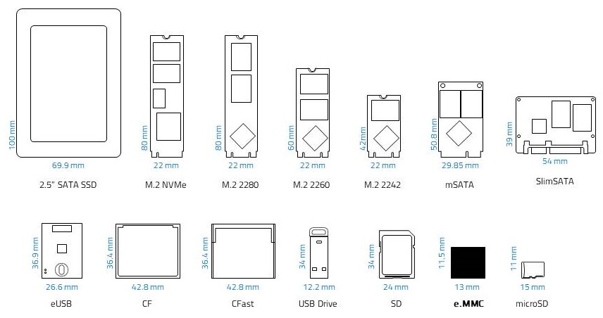
ATP industrial/automotive-grade e.MMC comes in a 153-ball Fine Pitch Ball Grid Array (FBGA) and is designed to meet high-performance data transfer, code and data storage requirements as well as automotive applications such as in-vehicle infotainment. As of this article’s publication (2020), the ATP e.MMC was constructed using 3D MLC NAND flash memory and achieved densities of up to 128 GB for use as mass storage.
The ATP e.MMC complies with JEDEC e.MMC standard v5.1 and is backward compatible with other e.MMC versions (v4.41/v4.5/v5.0). It supports features such as power-off notifications, packed commands, cache, boot or replay protected memory block (RPMB) partitions, high priority interrupt (HPI), and hardware (HW) reset.
ATP e.MMC Solutions
Specifications as of this article’s publication (April 2020); see the ATP e.MMC product page for current specifications.
| Specification | Premium (E700Pi) | Superior (E600Si) |
|---|---|---|
| IC Package | 153-ball FBGA | |
| JEDEC Specification | v5.1, HS400 | |
| Flash Type | 3D SLC Mode | 3D NAND |
| Density* | 8 GB to 64 GB | 16 GB to 128 GB |
| Bus Speed Modes | x1/x4/x8 | x1/x4/x8 |
| Performance** — Sequential Read/Write up to (MB/s) | 300/220 | 300/220 |
| Performance** — Random Read/Write up to (IOPS) | 15K / 30K | 15K / 30K |
| Operating Temperature | −40°C to 85°C (industrial) | |
| Reliability — Max. TBW** | 651 TB | 372 TB |
| Reliability — MTBF @ 25°C | > 2,000,000 Device hours | > 2,000,000 Device hours |
| VCC (Typical RMS in Read/Write) | 130 / 215 | 130 / 215 |
| VCCQ (Typical RMS in Read/Write) | 115 / 105 | 115 / 105 |
| L × W × H (mm) | 11.5 × 13.0 × 1.3 (max.) | |
Table 4. ATP industrial e.MMC specifications. * 1 GB = 1,000,000,000 bytes. Actual user storage may be less. ** Based on internal testing; performance may vary depending upon drive capacity, file attributes, host device, OS and application. Cache On.
Conclusion
e.MMC is a cost-effective, reliable embedded mass storage device that integrates the NAND flash memory, controller and interface in one package. ATP’s e.MMC solutions offer reliable storage for applications requiring high performance and endurance as well as low power consumption. Please visit the ATP e.MMC product page or contact an ATP Representative or Distributor in your area for more information.
Frequently Asked Questions (FAQ)
Q1: When should embedded systems use e.MMC instead of industrial SSDs?
A: Use e.MMC when the embedded system needs soldered-down storage for boot, application code, and local data at capacities up to 256 GB — especially where board space is tight, vibration is constant, or power is limited. ATP’s industrial e.MMC integrates NAND, controller, and interface in a 153-ball FBGA, operates from −40°C to 85°C, and provides up to 400 MB/s of HS400 bus bandwidth. An industrial SSD is the right choice when the workload needs more than 256 GB, sustained throughput beyond the e.MMC interface — SATA reaches 550 MB/s and PCIe NVMe goes higher — or a form factor that can be replaced in the field without board rework. Temperature rarely decides: industrial e.MMC and industrial SSDs share the −40°C to 85°C rating.
Q2: What is the difference between e.MMC and an SSD?
A: The difference is the level of integration, not the presence of flash management. e.MMC integrates NAND flash, a flash controller, and the MMC interface in one BGA package soldered to the host board; an SSD builds the same functional blocks — raw NAND chips managed by a discrete controller — onto a drive circuit board in form factors such as 2.5″, M.2, and mSATA. From the host’s perspective, both manage their own flash. Where they differ is interface and ceiling: e.MMC 5.1 tops out at 400 MB/s over HS400, while SATA SSDs reach 550 MB/s and PCIe NVMe SSDs go well beyond, at much higher maximum capacities.
Q3: Is e.MMC fast enough for embedded system boot and application storage?
A: For most embedded systems, yes. The e.MMC 5.1 HS400 interface provides up to 400 MB/s of bus bandwidth, and ATP’s industrial e.MMC is rated up to 310 MB/s sequential read and 240 MB/s sequential write, measured in ATP’s proprietary test environment without file system overhead. That covers OS boot, application loading, configuration data, and event or sensor logging with margin. It is not the right tool for sustained high-bitrate recording or large dataset processing — those workloads exceed the interface ceiling and point to an industrial SSD instead.
Q4: Does e.MMC handle wear leveling and error correction by itself?
A: Yes. e.MMC is managed NAND: the controller inside the package performs wear leveling, bad block management, and error correction internally, presenting the host with a simple block-storage device. The host needs no flash translation layer and spends no processor cycles on low-level flash maintenance — the main reason e.MMC simplifies embedded designs compared with raw NAND, which depends on the host or an external controller for all of those functions.
Q5: How much storage capacity does e.MMC support?
A: ATP’s current industrial e.MMC line spans 10 GB to 256 GB: 3D TLC configurations from 32 GB to 256 GB for capacity-oriented designs, and pSLC-mode configurations from 10 GB to 80 GB, which trade capacity for higher write endurance. A design that needs more than 256 GB has outgrown the e.MMC architecture; the step up is a soldered PCIe NVMe BGA SSD, which keeps the vibration-resistant BGA mounting, or a modular M.2 industrial SSD where the enclosure allows a socketed drive.