Power-loss protection (PLP) is a set of firmware and hardware mechanisms that ensure data and an SSD’s internal mapping tables survive an unexpected power cut. This article explains the four ways sudden power loss corrupts NAND flash storage, the four matching levels of PLP, and how ATP implements firmware-based SPOR and capacitor-backed HW+FW PLP on its industrial SSDs.
Key Takeaways
- Sudden power loss corrupts NAND flash storage in four distinct ways: data still in the volatile DRAM cache is lost outright; an interrupted program or erase operation leaves cells at indeterminate voltage levels that fail ECC on read; an interrupted write can damage previously stored data on the same page/block (data at rest); and in the worst case, a damaged mapping (linking) table makes the entire drive unreadable.
- Power-loss protection (PLP) is a set of firmware and hardware mechanisms that ensure data and the drive’s internal mapping tables survive an unexpected power cut. Modern SSDs implement it in four levels, from firmware backup (Level 1) to completing the last in-flight write with capacitor reserve power (Level 4).
- Firmware-only PLP (such as ATP Sudden Power-Off Recovery, SPOR) protects firmware, mapping tables, and data already at rest — but it cannot save data in flight. Only hardware PLP, with on-drive capacitors that power the last program/erase operation to completion, protects the data being written at the moment power is lost.
- PLP is not a substitute for system-level safeguards. It protects data inside the drive at the moment of power failure; data still in the host’s RAM or application buffers must be addressed by the system design (e.g., flush policies, UPS).
Why Are SSDs Vulnerable to Power Loss?
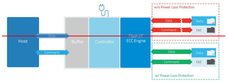
Solid state drives (SSDs) are particularly vulnerable to unstable power conditions and unexpected power interruptions. Unlike HDDs, SSDs do not have mechanical parts, so every component is electronic. The internal data management of an SSD involves many operations happening in the background, and every power loss or failure, no matter how short, can mean undue interruption of those operations, which could affect drive performance.
Data is typically written on the SSD in this order:
- The Host sends data to the SSD.
- The SSD Storage Controller acknowledges that data has been received.
- If the SSD does not have a DRAM cache, the Storage Controller moves the data to the NAND flash memory, which is non-volatile memory, so the data is safely stored even when power is terminated. If the SSD has a DRAM cache, the data is moved there first. This is volatile memory, so if power is terminated, the data is lost.
- The Storage Controller decides when to “Flush” the data from the DRAM cache to the NAND flash memory.
In a normal power shutdown, all data from the host is successfully transmitted to the NAND flash memory. Even if power is cut off, data remains there.
When power is terminated before data is moved or flushed into the SSD, the data may be corrupted or lost.
How Does Sudden Power Loss Corrupt NAND Flash Storage?
Sudden power loss corrupts NAND flash storage by interrupting operations that must complete atomically — and the damage is not limited to the data being written at that moment. There are four failure modes, and they map directly to the four protection levels described below:
- Loss of cached data. Data acknowledged by the controller but still sitting in the volatile DRAM cache disappears the instant power is cut. The host believes the data was saved; the NAND never received it.
- Interrupted program or erase operations. Programming a NAND page and erasing a block are multi-millisecond operations that raise cell voltages in steps. If power is cut mid-operation, the affected cells are left at intermediate threshold voltages — neither the old data nor the new — and subsequent reads fail ECC correction.
- Corruption of data at rest. Because NAND cells storing multiple bits share pages and word lines, an interrupted write can corrupt data that was successfully written earlier in the same page or block. This is why a power cut can damage files the user saved long before the event.
- Mapping (linking) table damage. The linking table is the index that maps the host’s logical block addresses to physical NAND pages. It is cached and rewritten to flash periodically; if power fails while updates are pending, the index — not just one file — is damaged. The worst case is a destroyed mapping table, which renders all data on the device inaccessible even though most NAND cells still hold valid data.
The four PLP levels exist precisely to close these four gaps: firmware backup guards the drive’s own code, linking-table backup guards the index, page/block protection guards data at rest, and capacitor-backed last-write protection guards data in flight. For a closer look at how industrial SSDs handle power instability, see ATP’s companion article.
Four Levels of Power-Loss Protection
Power-Loss Protection (PLP) mechanisms built into modern solid-state drives (SSDs) can be categorized into four levels:
Damaged Firmware Protection (Level 1). Multiple copies of the firmware (FW) are generated at different times to ensure a backup copy exists in case the master firmware gets corrupted. The master FW is always stored on the strongest flash pages and access is limited to reduce the possibility of read disturb, and to ensure both FW and data integrity.
Linking Table Damage Protection (Level 2). A NAND flash device creates a linking table to keep track of the physical flash pages with respect to the logical block addresses from the host. The linking table must be maintained and updated constantly so that the host can always access the most updated data via the two mapping addresses recorded on the flash device and the host.
The linking table is cached first and rewritten to the flash from time to time, so that the frequent index updating operation does not slow down the ongoing writing performance. When power disruption occurs while some mapping information is still in the flash cache, the mapping index is damaged, along with the data in the flash mapped by the respective linking table. The worst-case scenario is a destruction of the index table, resulting in the loss of all data in the storage device.
Multiple copies of the linking table are backed up for future restore situations when the linking table is distorted or lost during a sudden power loss, thus eliminating the risk of losing all data in a flash device as a result of losing the linking table.
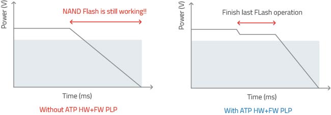
Page/Block Protection (Level 3). Data written on flash chips is divided into segments of millisecond-long operations. If power loss occurs and the writing process is interrupted at one segment point, for example the 8th millisecond, data error may occur when the host tries to access data that was already stored on the same page or block — data at rest. Level 3 protection guards previously written data on the affected page/block from corruption caused by the interrupted operation.

Last Write Page/Block Protection (Level 4). For SSDs with Level 4 protection, data in transit is secured by providing enough power to complete the last program operation before the power loss, guaranteeing that data is safely written onto the flash chip. In the illustration above, the last millisecond-long program operation is completed and data in the 8th segment is safely stored.
The following table summarizes the various levels of power protection to prevent data loss:
| Level | Description of Power Protection Levels |
|---|---|
| 4 (Most advanced) | Data-in-Flight, Last Page/Block Protection (for data being written onto the flash) |
| 3 | Data-at-Rest, Page/Block Protection |
| 2 | Index (Linking) Table Protection |
| 1 (Less advanced) | FW Protection |
ATP Sudden Power-Off Recovery (SPOR): Pure FW Power-Loss Protection
ATP Sudden Power-Off Recovery technology provides firmware-based PLP to minimize the effects of a sudden power off.
- ISP Code Backup. As soon as the device is powered On, the temporary in-system programming (ISP) code is generated in a spare block to reduce read access of the main ISP and to reduce the chances of read disturb.
- Link Table Mapping Address Backup. After power on, the FW will trace the link table from the latest mapping address. If the link table is found to be invalid, the FW will search the previous mapping address until the valid one is found. The mapping address is stored in a strong page only to ensure its integrity.
ATP’s HW + FW Power-Loss Protection Technology
It is critical to have a power-loss protection (PLP) mechanism, especially in high-performance computing environments where devices are running 24/7, the deployment is extensive, and data as well as device integrity could spell the difference between operational failure and success. Protecting stored data is just as crucial as protecting data in transit.
ATP integrates hardware design and firmware algorithms to defend against data loss at all four protection levels.
ATP harnesses the advantages of tantalum polymer capacitors, featuring low series resistance and minimal sensitivity to temperature and humidity. ATP SSDs with HW+FW PLP technology are designed for high reliability and endurance even in harsh environments. They also enable the HW+FW PLP mechanism to be implemented in small-size SSDs.
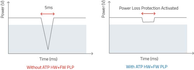
Upon sensing a power loss event, a power loss detection circuit integrated in the SSD immediately activates the power protection mechanism. The SSD then uses up reserve power from capacitors on the drive to complete the last Read, Write or Block Erase operation, while simultaneously stopping the controller from sending data to the flash chip to make sure that no data is lost in transit.
The following diagrams show how ATP’s HW+FW PLP prolongs the functionality of the NAND flash in two scenarios, allowing the SSD to complete the last command or data given by the controller.
The following table shows the typical and maximum amount of time for ATP’s HW+FW PLP to complete various commands during a power loss event.
| NAND Flash Operation | Typical | Maximum |
|---|---|---|
| Read (Page) | 76 (μs) | <120 (μs) |
| Program (Page) | 820 (μs) | <3500 (μs) |
| Erase (Block) | 15 (ms) | <30 (ms) |
| ATP’s HW+FW PLP holdup time | 50 (ms) | >80 (ms) |
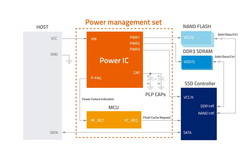
Microcontroller-Based PLP
Select ATP Serial ATA (SATA) and NVMe SSDs use a microcontroller unit (MCU) integrated into ATP HW+FW PLP. The design of the PLP array utilizes a power management IC (PMIC) and a firmware-programmable MCU that allow the PLP array to perform intelligently across various temperatures, power glitches and power states.
MCU-based PLP provides over input voltage protection, power-up inrush current suppression, input power noise de-glitch, fast power on-off control, PLP capacitors over voltage protection, and customization options.
For more information on MCU-based PLP, please visit this page.
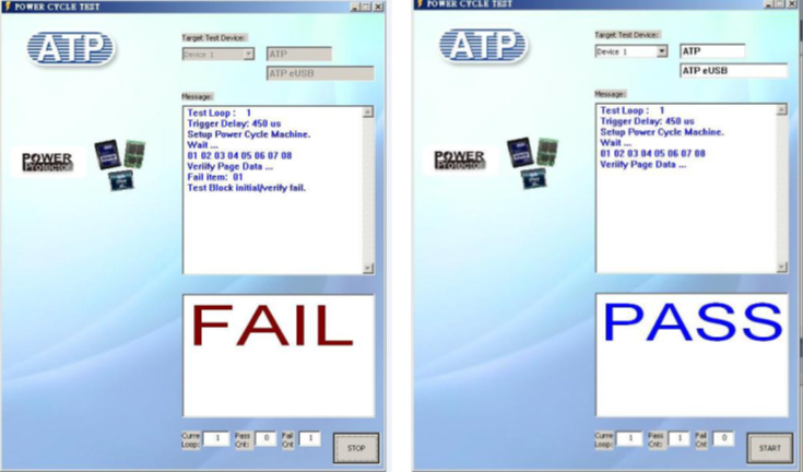
ATP Power Cycling Tester
ATP’s own-built power cycling tester validates the design of the PLP mechanism under sudden power-off conditions. At the beginning of each cycle, the power tester writes a segment of data pattern onto the SSD test device. Power is then cut off at the exact configured millisecond while data is being programmed into the NAND flash blocks. By creating a sudden power failure at the “write” command stage, the test proves the effectivity of the PLP mechanism, showing a “Pass” over thousands of power cycles without any data errors.
During the Power Cycling Test, a window of time for a device without ATP HW+FW PLP is evident during the specific time frame in milliseconds when data loss is most likely to occur with a power glitch. This finding is critical for product development teams to fine tune the programming of future NAND flash products with their host systems.
The following figures show that a product without the ATP HW+FW PLP will have corrupted data and a “Fail” result due to data miscompare in the post-test check conducted after each power cycle. The product with ATP HW+FW PLP shows a “Pass” result without any data loss.
Conclusion
ATP offers both firmware and hardware solutions aimed at protecting valuable data on an SSD. ATP HW+FW PLP offers advanced power-loss protection to ensure data integrity even during a power failure scenario and to preserve data in mission-critical applications. The PLP mechanism features a standalone design, solid-state capacitors, and long life span.
For SSDs with ATP’s MCU-based PLP, the power-loss protection adds intelligent power management beyond basic backup approaches. Moreover, ATP’s Power Cycling Tester, which removes power at the exact millisecond during the programming of the NAND flash product, further validates and improves ATP product lines’ overall reliability.
For more information on ATP HW+FW PLP and other power-loss protection technologies, visit the ATP website or contact an ATP Representative.
Frequently Asked Questions (FAQ)
Q1: What is power-loss protection (PLP) on an SSD?
A: Power-loss protection (PLP) is a set of firmware and hardware mechanisms that ensure data and the drive’s internal mapping tables survive an unexpected power cut. Modern SSDs implement it at four levels: firmware backup, mapping (linking) table backup, page/block protection for data at rest, and capacitor-backed completion of the last in-flight write. The first three can be implemented in firmware alone; the fourth requires reserve power from on-drive capacitors.
Q2: How does sudden power loss corrupt NAND flash storage?
A: Power loss corrupts NAND flash in four ways: data still in the volatile cache is lost before it reaches the NAND; an interrupted program or erase leaves cells at intermediate voltages that fail ECC on read; an interrupted write can also damage previously stored data sharing the same page or block; and a damaged mapping table can make every file on the device inaccessible, even though the underlying cells are intact.
Q3: Can a power failure damage data that was already saved successfully?
A: Yes. Because NAND cells storing multiple bits share pages and word lines, a write interrupted by power loss can corrupt data written earlier in the same page or block — this is data-at-rest corruption, and it is what Level 3 (page/block) protection addresses. Mapping-table damage is the other path: the old data is physically intact but the index pointing to it is lost.
Q4: Does firmware-based power-loss protection save data that is being written when power fails?
A: No. Firmware-based PLP such as ATP’s Sudden Power-Off Recovery (SPOR) protects the firmware, the mapping table, and data already at rest, and recovers the drive to a consistent state on the next power-up — but data in flight at the instant of power loss is lost. Completing the last write requires hardware PLP: capacitors on the drive that supply reserve power until the final program or erase operation finishes. ATP implements capacitor-backed HW+FW PLP across its industrial SATA and NVMe SSDs.