DRAM fundamentals are the handful of concepts — chip density and configuration, data width, rank, and ECC — that let you read any memory module specification and know exactly what is on the board, how the chips are grouped, and whether the module corrects errors.
Key Takeaways
- A DRAM chip’s notation, such as “2Gx8,” encodes its depth and its data width. The 2G is the number of addressable storage locations (2 billion); the x8 is the data-bus width (8 bits per access). Multiply them and you get the chip’s density: 2G × 8 = 16 gigabits (Gb).
- Data width determines how many chips it takes to fill a memory channel. A standard channel is 64 bits wide, so it takes eight x8 chips, four x16 chips, or sixteen x4 chips to fill one rank — which is why width drives module capacity, ECC layout, and power.
- A rank is an electrical group of chips that together fill the data bus, not a measure of speed. A dual-rank (2R) module holds two independent groups sharing one 64-bit bus; the controller talks to one rank at a time using a separate Chip Select signal for each.
- ECC memory is wider memory. DDR2 through DDR4 ECC modules run a 72-bit bus instead of 64-bit; DDR5 adds check bits inside each sub-channel. The extra width means extra chips — and registered DIMMs (RDIMMs) are always ECC by design.
- DDR5 relocated several functions onto the die and the module. On-die ECC, a per-module power management IC (PMIC), 32 internal banks across 8 bank groups, and a 16n prefetch all change how you read a DDR5 datasheet compared with DDR4.
What a DRAM spec actually describes
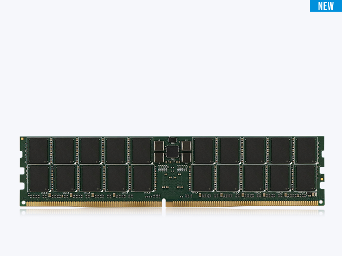
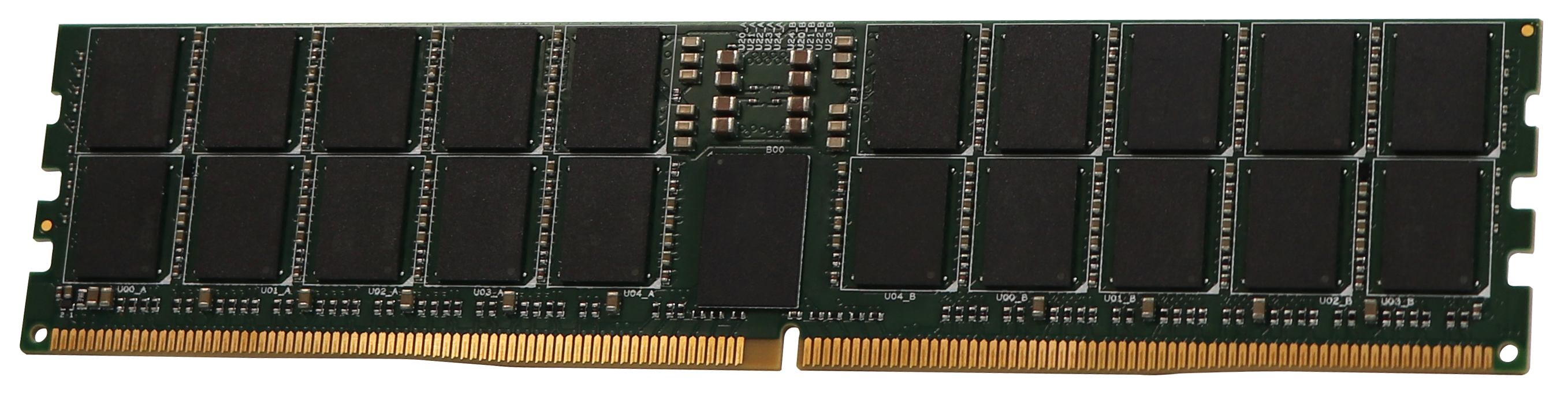
You are comparing two memory modules with the same capacity on the label, yet one reads 1Rx8, another 2Rx8, and a third stacks on ECC UDIMM with a module organization of 2Gx80. That shorthand is the vocabulary DRAM uses to describe itself. None of it is decoration. Each term maps to a physical decision — how many chips are on the board, how wide each one is, how they are grouped electrically, and whether the module carries error correction.
This guide walks through the fundamentals an engineer or technical buyer needs to read a DRAM module specification with confidence: chip density and configuration, the x8-versus-x16 choice, what you can and cannot mix, memory rank, ECC, and the specifics that DDR5 introduced. Each section links to a deeper article in this series. Think of this page as the map; the satellite posts are the detailed routes.
What a configuration like “2Gx8” actually tells you
A DRAM chip’s configuration describes its internal organization in two numbers: depth and width. The depth (the 2G in 2Gx8) is the number of addressable storage locations on the chip — here, 2 billion. The width (the x8) is the data-bus width, meaning the chip reads or writes 8 bits per access.
Multiply depth by width and you get density, the total number of bits the chip stores: 2 billion locations × 8 bits = 16 gigabits. So a 2Gx8 part is a 16 Gb chip. Keep two units straight here — density is measured in gigabits (Gb) per chip, while module capacity is measured in gigabytes (GB). Confusing the two is a common spec-reading error — and an easy one to avoid.
For the full breakdown, including how the same density appears in different width options, see the density and configuration article.
x8 vs x16: why the same capacity is built two ways
Two chips can hold identical density and still be organized differently. A 4Gx8 chip and a 2Gx16 chip are both 32 Gb — but one is 8 bits wide and the other is 16. That difference decides how many chips a module needs.
Because a standard channel is 64 bits wide, you fill one rank with eight x8 chips or four x16 chips. The x8 path is the standard for high-capacity and server memory: eight chips fill the channel, and adding a ninth (or tenth) chip provides ECC cleanly. The x16 path uses fewer chips, which saves board space and power — the reason it dominates laptops, SO-DIMMs, and compact embedded designs. There is also a modest performance dimension, because x8 devices typically expose more bank groups than x16 parts of the same generation.
The full tradeoff — capacity, ECC, space, power, and bank-level parallelism — is covered in the x8 vs x16 article.
What a module and a channel will tolerate when you mix parts
You cannot mix different chip depths or widths on a single DIMM. The address bus, the data-trace routing, and the registering clock driver on a registered module are all wired for one specific configuration. A x16 chip will not function on a PCB whose traces route 8 data bits to each chip site.
Across slots, the rules loosen but do not disappear. Some consumer motherboards accept mismatched modules and quietly downclock to the slowest common module — or fail to train. Server platforms are far stricter: a memory channel, and often the entire processor, typically requires every DIMM to share the same rank count and data width.
The mixing rules — on a module and across a channel — are detailed in the mixing configurations article.
Rank: single rank versus dual rank
A memory rank is an electrical grouping of DRAM chips that work together as one set to fill the system’s full data-bus width — 64 bits for standard memory, or 72/80 bits for ECC. A single-rank (1R) module has one such group. A dual-rank (2R) module has two independent groups wired in parallel onto the same data bus.
Because both ranks share the same data wires, they cannot transmit at the same time. The memory controller manages this with a Chip Select (CS) signal — one per rank — activating one rank while the other idles or precharges. The practical effect: at the same width, a 2R module roughly doubles capacity over a 1R module, and the extra rank can improve parallelism, with a small signal-loading cost at the highest speeds.
Single rank versus dual rank, Chip Select, and the capacity math are explained in the memory rank article.
ECC: on-die, module-level, and why RDIMMs are always ECC
Error Correction Code (ECC) appears in two distinct forms in the DDR5 era, and they are easy to conflate. On-die ECC corrects errors inside the DRAM chip before data leaves it; every DDR5 chip includes it by JEDEC mandate, primarily to sustain yield and reliability as memory cells shrink. It does not protect the data once it travels across the module and the motherboard to the central processing unit (CPU).
Module-level ECC — the kind servers have always used — protects that full path. It requires extra bus width and therefore extra chips, which is why a registered DIMM (RDIMM), built for servers and workstations, is always an ECC module. The two mechanisms are complementary, not interchangeable.
The full comparison, plus the chip-count math behind ECC modules, is in the DDR5 ECC article.
Reading a DDR5 datasheet
DDR5 carried over the fundamentals above but moved several functions onto the die and the module. A datasheet now reports a module organization that includes ECC bits in its bus width, an on-module power management IC, on-die ECC, 32 internal banks organized into 8 bank groups, a 16n prefetch with a default burst length of 16, and refresh behavior that tightens with temperature.
If you are interpreting timing parameters, prefetch, bank organization, ZQ calibration, and power and refresh behavior at the level a design engineer needs, the DDR5 datasheet deep-dive walks through each field.
Putting it together
Read a module spec from the chip outward. The configuration (e.g., x8) tells you the chip’s width; density (in Gb) times the chip count gives module capacity (in GB); the rank count tells you how those chips are grouped electrically; and the ECC designation tells you whether the bus is widened for error correction and whether a register is present. Once those four facts are in hand, a label like “2Rx8 32GB ECC UDIMM” stops being a code and starts being a description.
ATP designs and validates DRAM modules for industrial and embedded systems — including wide-temperature operation and edge-AI platforms, where a module has to hold its rating well outside a desktop’s comfort zone. Reading a spec correctly matters more, not less, when the deployment runs unattended for years. Each linked article goes one level deeper.
Frequently Asked Questions (FAQ)
Q1: What is the difference between density and capacity in DRAM?
A: Density is the storage of a single DRAM chip, measured in gigabits (Gb); capacity is the storage of the whole module, measured in gigabytes (GB). Module capacity equals chip density times the number of chips, divided by eight to convert bits to bytes. A 16 Gb chip contributes 2 GB to a module.
Q2: How do I read a label like 2Rx8?
A: The 2R means dual rank — two independent groups of chips on the module. The x8 means each DRAM chip is 8 bits wide. Together they tell you the module has two ranks of eight 8-bit chips (16 chips total) sharing one 64-bit data bus.
Q3: Does ECC memory make my system slower?
A: Module-level ECC adds a small, usually negligible latency because the controller verifies check bits, and ECC modules carry extra chips that add minor electrical load. In the systems that require ECC — servers, workstations, and other always-correct environments — the reliability benefit outweighs the marginal cost.
Q4: Is every DDR5 module an ECC module because DDR5 has on-die ECC?
A: No. On-die ECC is built into every DDR5 chip, but it only protects data inside the chip. Module-level ECC, which protects the path to the CPU, is still a separate feature found on ECC UDIMMs, ECC SODIMMs, and all RDIMMs.
Q5: Why does a 64-bit channel need eight x8 chips?
A: Each x8 chip contributes 8 bits to the data bus. Eight chips × 8 bits = 64 bits, which fills one standard channel as a single rank. With x16 chips you need only four; with x4 chips you need sixteen.